Next Generation Organic Substrate Technology: How Will it Synergize with 2.5D?
![]() Omar Bchir, Qualcomm Omar Bchir, Qualcomm
 ABSTRACT: As chiplet packaging proliferates, a reduction in die interconnect pitch and concomitant increase in escape routing density must be enabled to meet performance and cost targets. The traditional 2D solution (die on organic substrate) has limitations related to pitch and escape routing capability, which have promoted a shift to 2.5D technology (die + high density routing interface + organic substrate) in certain application spaces. Conventional thought is that use of a 2.5D solution can enable coarser, lower cost substrate design rules. However, a different cost point for 2D vs. 2.5D means that interconnect and escape routing should be properly balanced between the organic substrate and the high-density routing interface, to contain cost while delivering the proper level of chiplet integration. As both 2D and 2.5D solutions include an organic substrate, continuous development of higher routing density organic substrates is a prudent approach to enable cost-optimized solutions moving forward. This talk will cover current application space and limitations for 2D vs. 2.5D technology, and potential paths forward to achieve a cost-optimized, complementary solution. ABSTRACT: As chiplet packaging proliferates, a reduction in die interconnect pitch and concomitant increase in escape routing density must be enabled to meet performance and cost targets. The traditional 2D solution (die on organic substrate) has limitations related to pitch and escape routing capability, which have promoted a shift to 2.5D technology (die + high density routing interface + organic substrate) in certain application spaces. Conventional thought is that use of a 2.5D solution can enable coarser, lower cost substrate design rules. However, a different cost point for 2D vs. 2.5D means that interconnect and escape routing should be properly balanced between the organic substrate and the high-density routing interface, to contain cost while delivering the proper level of chiplet integration. As both 2D and 2.5D solutions include an organic substrate, continuous development of higher routing density organic substrates is a prudent approach to enable cost-optimized solutions moving forward. This talk will cover current application space and limitations for 2D vs. 2.5D technology, and potential paths forward to achieve a cost-optimized, complementary solution.
Bio: Omar Bchir has worked in the field of IC packaging for 20 years. He joined Intel Corporation in 2004 as a Substrate Pathfinding Engineer. In 2008, he moved to Qualcomm, where he remained for eight years, forming a substrate team and eventually leading the Advanced Packaging team. In 2016, Omar joined Rockley Photonics, focusing on design and proof of concept for next-generation Opto-ASIC network switches for mega data centers. In 2017, he joined Micron Technology, focusing on memory packaging development and optimization for automotive customers. In 2020, Omar joined Amazon’s Project Kuiper, developing packages for terrestrial and space-based applications to support low-latency, high bandwidth satellite-based broadband internet access. Omar re-joined Qualcomm in 2023, and currently leads the Substrate and Module Systems Engineering Team. Omar received a B.S. degree in chemical engineering from the Georgia Institute of Technology, and a Ph.D. degree in chemical engineering from the University of Florida. He holds 42 issued U.S. patents and has authored 13 publications.
|
|
Advanced Photo-imageable Dielectric Film Enabling Sub-5-micron Patterning for Next-Generation Build-up Layer
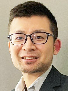 Hikaru Mizuno, JSR Micro Hikaru Mizuno, JSR Micro
ABSTRACT: As novel electronic products become dramatically smaller and more highly functionalized, semiconductor packaging structures are also required to become smaller, thinner and more complicated. Based on these market trends, the IC substrate has become one of the most important components in packaging. Next-generation build-up layer patterning materials for IC substrates are required to meet the demands of ultra-fine via patterning … (smaller than 5 micron) while also providing good thermomechanical properties such as a low coefficient of thermal expansion (CTE). In this presentation, we report our development approach and the performance of a novel photo imageable dielectric (PID) film material. The PID film shows a nearly vertical pattern profile with a sidewall taper angle of >85°, for 6 µm via features at 20 µm thickness. Small features of ?5 µm-via are also achievable at 10µm thickness. The thermal property of the PID film has a Tg of 260? and a CTE of 31 ppm/? after cure at 200?. Peel strength of plated Cu shows 0.38 N/mm for initial, and 0.46 N/mm after unbiased highly accelerated stress test (uHAST). Those properties meet typical requirements of a build-up material. It’s suggested that the novel PID film is a promising material for next generation build-up layers.
Bio: Hikaru Mizuno joined JSR Corporation in 2009 and worked in Fine Electronic Materials Research Laboratories. In 2018, he joined JSR Micro, Inc., and has been engaged in research and development of electronic materials especially RDL related materials. He has submitted 9 papers and 18 patents.
|
Dry-film Solder Resist Materials for high density IC Substrates
![]() Yuya Suzuki, Taiyo America Yuya Suzuki, Taiyo America
 ABSTRACT: The demand for high-density integrated circuit (IC) substrates is driving advancements in material technologies to meet the increasing complexity and performance requirements of high-performance electronics. Solder resist (SR) materials play a critical role in IC substrate applications by providing insulation and protecting circuit patterns … from environmental and mechanical damage. Specifically, dry-film solder resist (DFSR) offers various benefits for advanced packaging, including refined thickness control, small-pitch opening capability, and excellent insulating reliability. These features enable DFSR to support precise electrical connections without signal interference while ensuring the integrity of fine-pitch designs. ABSTRACT: The demand for high-density integrated circuit (IC) substrates is driving advancements in material technologies to meet the increasing complexity and performance requirements of high-performance electronics. Solder resist (SR) materials play a critical role in IC substrate applications by providing insulation and protecting circuit patterns … from environmental and mechanical damage. Specifically, dry-film solder resist (DFSR) offers various benefits for advanced packaging, including refined thickness control, small-pitch opening capability, and excellent insulating reliability. These features enable DFSR to support precise electrical connections without signal interference while ensuring the integrity of fine-pitch designs.
This talk explores recent innovations in DFSR materials tailored for high-density IC substrate applications and examines material trends for next-generation technologies.
Bio: Dr. Yuya Suzuki is a technical marketing manager of Taiyo America. He has a Ph.D. degree in materials science from Georgia Tech, and has more than 15 years of experience in electronic materials for advanced IC packaging. Dr. Suzuki has published more than 30 papers in scientific journals and conferences.
|
|
Advanced Insulation Material for High Performance Semiconductor Packages
 Shiro Tatsumi, Ajinomoto Shiro Tatsumi, Ajinomoto
ABSTRACT: Printed circuit boards such as multi-layer printed wiring boards and flexible printed wiring boards are used for a wide variety of electronic devices. Ajinomoto Build-up Film®(ABF) has been widely utilized for a variety of package structures due to its outstanding insulation reliability, good resin flow, thickness uniformity and Semi-Additive Process (SAP) compatibility for fine line and space formation. Low coefficient of thermal expansion (CTE) and low transmission loss (Df) for high-speed applications are crucial for ABF qualities, in addition to the growing needs for larger packages. GL series were created as new ABFs for next-generation packages to satisfy these requirements.
Due to glass’s superior mechanical and electrical stability as well as its superior flatness, glass substrates have recently drawn the attention of package trends. These characteristics would help next-generation packages achieve lower energy consumption and higher density connectivity. Large packages with a high number of layers are also necessary for high performance computing applications to meet the demands of the rapidly expanding server and AI technologies. New ABF with low CTE (less than or equal to 17 ppm) and low Df (less than or equal to 0.003) was created to satisfy the requirements. minimal transmission loss is also a result of the new ABF’s minimal surface roughness, even after the desmear chemical etching procedure. These findings demonstrated that New ABF would meet the possible needs of upcoming package trends. Furthermore, nano-sized filler ABF (Nano filler ABF) was created to meet the high demands for ultra-thin layer to layer structure, small via, and fine line and space. To achieve the same performance as traditional ABF, nano filler ABF was developed with a maximum loaded silica filler size of less than 1 um. It helps create a smooth surface and an ultra-thin resin layer, which makes it possible to fabricate fine via, lines, and spaces. It was shown that employing the nano filler ABF, 2/2um line and space formation could be accomplished. Several techniques, including deep ultraviolet laser via, excimer laser via, plasma via, and Cu pillar, were used to study small via manufacturing. The latter, commonly known as the via-less technique, would need CMP following encapsulation with ABF, a nano filler. Using these via opening techniques, a via with a smooth via side wall shape and a diameter of less than 5 um was successfully opened. High density connectivity for FOWLP and FOPLP applications is made possible by these small via patterning techniques.
Bio: (to be supplied)
|
DGlass Compositions for Data Centers, AI, and Quantum Computing
![]() Vern Stygar, AGC Vern Stygar, AGC
 ABSTRACT: The use of glass as a core material for electronic and photonic packaging substrates is being considered due to its rigidity, flatness, and dimensional stability for advanced packaging such as chiplet packaging requiring large format and high-density interconnection. This presentation will provide an overview of glass material technology, processing technology and the need for reliability testing for glass core substrates. ABSTRACT: The use of glass as a core material for electronic and photonic packaging substrates is being considered due to its rigidity, flatness, and dimensional stability for advanced packaging such as chiplet packaging requiring large format and high-density interconnection. This presentation will provide an overview of glass material technology, processing technology and the need for reliability testing for glass core substrates.
Bio: Vern Stygar has worked in the semiconductor industry for more than 35 years and began his career as a process engineer at Beckman Instruments followed by 10 years at Ferro Corporation as the product manager for thick film paste and LTCC for high-frequency devices. In 2004 Vern joined AGC as the product manager for glass for semiconductor products. In his role as a product manager, Vern is responsible for advanced packaging for High Frequency products, co-packaged photonics and structured glass. Vern has authored or co-authored papers for high frequency applications utilizing glass, thick film and thin film metallization. Vern holds a degree in Chemistry and an MBA.
|
|
The Development of Organic Substrate Materials for Advanced Packaging
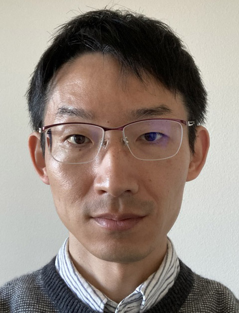 Masa Fukui, Resonac America, Inc. Masa Fukui, Resonac America, Inc.
ABSTRACT: The development of advanced packaging technology has been accelerated, such as 2.5D packaging and chiplet design. Advanced packaging requires HSIO, high density interconnection and large form factor. This motivation for future packaging is the driving force behind the development of substrate materials to meet the challenges. In this perspective, glass substrates are considered as the future generation substrate, while at the same time, the development of glass-like organic substrates is accelerating. Organic substrate materials including prepreg and resin sheets with superior physical properties can be made thinner while maintaining warpage, thereby enabling fine pitch through-hole and reducing signal loss. Coplanarity, dimensional stability and small thickness variation are required to improve manufacturing yields for large size packages. The latest development on and technical direction for organic substrate materials will be presented.
Bio: Masa Fukui received his degree of Master of Engineering in Molecular Chemistry and Applied Chemistry from Osaka University’s Graduate School of Engineering. He joined Hitachi Chemical Co., Ltd. since 2007 which was later consolidated into Resonac Corp. He worked as an engineer in the Laminate Materials R&D department. Masa joined Resonac America, Inc. in October 2022.
|
DUCIe 2.0: Open Chiplet Innovation Continues with Vertical and Planar Connectivity
![]() Debendra Das Sharma, Intel Debendra Das Sharma, Intel
 ABSTRACT: High-performance workloads demand on-package integration of heterogeneous processing units, on-package memory, and communication infrastructure such as co-packaged optics to meet the demands of the supercomputing landscape. On-package interconnects are a critical component to deliver the power-efficient performance with the right feature set in this evolving landscape. ABSTRACT: High-performance workloads demand on-package integration of heterogeneous processing units, on-package memory, and communication infrastructure such as co-packaged optics to meet the demands of the supercomputing landscape. On-package interconnects are a critical component to deliver the power-efficient performance with the right feature set in this evolving landscape.
Universal Chiplet Interconnect Express (UCIe), is an open industry standard with a fully specified stack that comprehends plug-and-play interoperability of chiplets on a package; like the seamless interoperability on board with well-established and successful off-package interconnect standards such PCI Express® and Compute Express Link (CXL)®. In this talk, we will discuss the usages and key metrics associated with different technology choices in the second generation of UCIe (UCIe 2.0), supporting both planar and vertical interconnects, and how it addresses the manageability, test, and debug challenges of heterogeneous chiplets on package.
Bio: Dr. Debendra Das Sharma is an Intel Senior Fellow and Chief I/O Architect, Data Platforms and Artificial Intelligence Group. He is a leading expert on I/O subsystem and interface architecture. He delivers Intel-wide critical interconnect technologies in Peripheral Component Interconnect Express (PCIe), Compute Express Link (CXL), Universal Chiplet Interconnect Express (UCIe), and Intel’s Coherency interconnect, as well as their implementation.
Dr. Das Sharma is a member of the Board of Directors and treasurer for the PCI Special Interest Group (PCI-SIG). He has been a lead contributor to PCIe specifications since its inception. He is the co-inventor of CXL, a founding member of the CXL consortium, and chairs the CXL consortium. He co-led the CXL Board Technical Task Force (2019-2024), and is a leading contributor to CXL specifications. He co-invented the chiplet interconnect standard UCIe and is the chair of the UCIe consortium. He has a Ph.D. in Computer Engineering from the University of Massachusetts, Amherst, and holds 190+ US patents and 500+ patents world-wide. He received the IEEE Region 6 Outstanding Engineer Award in 2021, the first PCI-SIG Lifetime Contribution Award in 2022, the IEEE Circuits and Systems Industrial Pioneer Award in 2022, and the IEEE Computer Society Edward J. McCluskey Technical Achievement Award in 2024.
|
|
  Jason Conrad, Chief Operating Officer, ASU Knowledge Enterprise, and Craig Bishop, Chief Technology Officer, Deca Technologies Jason Conrad, Chief Operating Officer, ASU Knowledge Enterprise, and Craig Bishop, Chief Technology Officer, Deca Technologies
ABSTRACT: The CHIPS Act renewed a domestic focus on semiconductor technology, including advanced packaging that is critical for chiplets and future scaling. Under the National Advanced Packaging Manufacturing Program (NAPMP), ASU is leading the Substrate-based Heterogeneous Integration Enabling Leadership Demonstration for the USA (SHIELD USA) program in collaboration with Deca Technologies and major industry partners, to rethink how organic substrates are manufactured. Processes, materials, and equipment borrowed from fan-out wafer-level and panel-level packaging will enable scaling down to features sizes that are only available on interposers today and scaling out to 100s-1000s of chiplets. As dimensions and features on organic substrates push beyond state-of-the-art and converge toward silicon-like capabilities, many challenges arise. SHIELD USA will address these challenges and de-risk 600mm panel processing for molded-core organic substrates.
Bio: Jason Conrad is Arizona State University’s SWAP Hub’s Chief Operating Officer, and brings with him more than 23 years of experience in the semiconductor industry from wafering and silicon machining to wafer fabrication for both silicon CMOS and wide bandgap semiconductors. With previous roles at industry-leading companies such as NXP Semiconductors, Global Wafers, and Lam Research, Jason is a proven leader focused on performance and quality who has long served as a bridge between technical and non-technical personnel.
He is also the Site Lead for MacroTechnology Works, ASU’s premier facility for semiconductor research and development. His passion for optimizing manufacturing processes and improving efficiency serve him well in these roles. Jason’s mission is to foster relationships with academic, industry and government partners to not only develop leap ahead technologies but also to develop the workforce of the future. Jason holds a bachelor’s degree in chemical engineering from the University of Notre Dame. He earned a Six Sigma Green Belt along with significant experience in lean manufacturing and project management.
|
Complexity Handling of Integrated Circuits Design Using AI-based EDA Technology with Smart Substrates
![]() Dr. John Damoulakis, Sr. Director – Advanced Technology Programs at Cadence Design Systems Dr. John Damoulakis, Sr. Director – Advanced Technology Programs at Cadence Design Systems
 ABSTRACT: The advent of microelectronics technology evolution has from one hand created numerous market opportunities for applications in high-performance-computing (e.g., data centers) and ultra-low-power (e.g., biomedical, automotive, etc.) electronics that were not possible before, but on the other hand has created substantial complexity in the design, manufacturing, packaging, and testing of either 2D, or 2.5D, or 3D integrated circuits (ICs). This complexity introduces repeated tapeouts that is the main cause of increased cost and product delays to market. There are potential remedies to alleviate these complexities. First, some standard circuitry can be embedded in substrates (e.g., part of power distribution, part of communication fabric, etc.) making them smart substrates, which not only may alleviate some of the circuitry complexity in the IC’s tiers, but also minimize the design needs of interposers. And second, EDA tools empowered by artificial intelligence (AI) that can help to deal with the IC’s design complexity issues. Together, these approaches can potentially accelerate the design, manufacturing, packaging, and testing turn-around-time (TAT) and reduce developmental cost. This talk addresses these issues and presents potential design approaches that could offer high payoff. ABSTRACT: The advent of microelectronics technology evolution has from one hand created numerous market opportunities for applications in high-performance-computing (e.g., data centers) and ultra-low-power (e.g., biomedical, automotive, etc.) electronics that were not possible before, but on the other hand has created substantial complexity in the design, manufacturing, packaging, and testing of either 2D, or 2.5D, or 3D integrated circuits (ICs). This complexity introduces repeated tapeouts that is the main cause of increased cost and product delays to market. There are potential remedies to alleviate these complexities. First, some standard circuitry can be embedded in substrates (e.g., part of power distribution, part of communication fabric, etc.) making them smart substrates, which not only may alleviate some of the circuitry complexity in the IC’s tiers, but also minimize the design needs of interposers. And second, EDA tools empowered by artificial intelligence (AI) that can help to deal with the IC’s design complexity issues. Together, these approaches can potentially accelerate the design, manufacturing, packaging, and testing turn-around-time (TAT) and reduce developmental cost. This talk addresses these issues and presents potential design approaches that could offer high payoff.
Bio: Dr. John N. Damoulakis is a Sr. Director – Advanced Technology Programs at Cadence Design Systems. In that position, he focuses to bring together into an integrated framework/approach, Cadence’s core technologies on electronic design automation (EDA), simulation, emulation, and digital twinning (DT) tools to address the technology challenges encountered on information sciences, microelectronics, knowledge-based algorithms, and signal processing application domains. This involves not only the design of various domain-specific electronic components (digital, analog, photonics, etc.), but also packaging and testing, especially those involving heterogeneous functionality and materials. He holds a Ph.D. from Rice University, Houston, Texas, in ME, and a MS in EE and ME from the Technical University of Athens, Athens, Greece.
Dr. Damoulakis has over 30 years of experience in concept definition, development, transition to operational systems, and management of high-technology programs for the commercial and defense industries. Prior to Cadence, Dr. Damoulakis was at the University of Southern California’s (USC’s) Information Sciences Institute (ISI) as a Sr. Director and Director of Advanced Electronics, and prior he was a Sr. Director at Lockheed-Martin developing a variety of electronic systems, and was also, responsible for the research and development of many divisions within the corporation. He is often a consultant to many governmental agencies as a subject-matter-expert within the areas of his expertise. He is the author of numerous technical papers in the areas of engineering sciences and holds four patents. He is the recipient of the Franklin’s Institute Levy medal for his contributions to optimal control and estimation (1973), and USC’s ISI award of excellence for exceptional contributions (2019).
|
|
(to be supplied)
 Craig Bishop, Chief Technology Officer, Deca Technologies Craig Bishop, Chief Technology Officer, Deca Technologies
ABSTRACT:
Bio: Craig Bishop is Chief Technology Officer at Deca Technologies, managing the Adaptive Patterning technology, EDA development, intellectual property, and R&D. He is also Technical Director for the $100M SHIELD USA program in close collaboration with ASU to produce leap-ahead organic substrates under the National Advanced Packaging Manufacturing Program (NAPMP). Prior, Craig was the architect of Adaptive Patterning at Deca where he developed the technology and design methodologies that have been implemented in high-volume production, with over seven billion devices shipped in leading smartphones and other electronics. Craig Bishop received his B.S. degree in electrical and computer engineering from the University of Arizona in Tucson with specialization in analog IC design. He has over than two dozen patents issued related to fan-out and electronic interconnects.
|
Wafer-Level Si Core substrates – Third Leg of the NAPMP Substrates Program
![]() Steven Verhaverbeke, Applied Materials Steven Verhaverbeke, Applied Materials
 ABSTRACT: The rise of chiplet and 2.5D packaging has been driven by the increasing demands for higher performance, scalability, and power efficiency in modern semiconductor design. As Moore’s Law slows, traditional monolithic scaling becomes less viable due to cost and yield challenges. 2.5D packaging, which utilizes an interposer to connect multiple chiplets, has emerged as a key enabler by providing high-bandwidth, low-latency interconnects while mitigating signal integrity and power delivery challenges. This approach is widely adopted in AI accelerators, high-performance computing (HPC), and networking applications, offering a path to scaling performance without the complexity of full 3D stacking. ABSTRACT: The rise of chiplet and 2.5D packaging has been driven by the increasing demands for higher performance, scalability, and power efficiency in modern semiconductor design. As Moore’s Law slows, traditional monolithic scaling becomes less viable due to cost and yield challenges. 2.5D packaging, which utilizes an interposer to connect multiple chiplets, has emerged as a key enabler by providing high-bandwidth, low-latency interconnects while mitigating signal integrity and power delivery challenges. This approach is widely adopted in AI accelerators, high-performance computing (HPC), and networking applications, offering a path to scaling performance without the complexity of full 3D stacking.
2.5D silicon interposer packaging, while enabling high-bandwidth chiplet integration, comes with several limitations and challenges. A primary constraint is reticle size, which restricts the maximum interposer dimensions, limiting scalability for large and complex designs. Signal integrity issues also emerge as longer interconnects, increased parasitic effects and multiple transition layers introduce latency and degrade high-speed signal performance. These challenges drive the search for alternative approaches, such as silicon core substrates, which aim to simplify integration while improving performance, yield, and cost efficiency.
A multilayer silicon core substrate allows direct high-density routing of chiplet connections without the need for a separate interposer. This reduces signal integrity issues by minimizing interconnect length, lowering parasitics, and improving power delivery. Reliability is also enhanced, as eliminating the interposer reduces mechanical stress, thermal expansion mismatches, and potential failure points. Additionally, testing and manufacturability are simplified, as the silicon core substrate supports direct integration of chiplets, improving yield and fault isolation. This approach enables scalable, high-performance chiplet architectures while overcoming the limitations of traditional 2.5D integration.
Bio:
|
|
The Latest Vacuum Lamination Challenges and Technology Development
 Yoshihiro Inoue, Nikko-Materials Yoshihiro Inoue, Nikko-Materials
ABSTRACT: This talk will cover essentials of the vacuum lamination process for the lamination of film materials, introducing NM’s widely applicable vacuum laminator with lamination process towards uneven surface with detail pattern and the function of flattening uneven surfaces. Also discussed will be the diverse processes for vacuum laminator in response to the growth of IC packaging, and the capability processes of the NM vacuum laminator.
Bio: Yoshihiro Inoue has experience developing film laminate processes for vacuum laminators, with additional experience from supplier process development to equipment application. He has worked on process development in the IC substrate field.
|
Large Scale Glass substrate for High Performance
![]() Satoru Kuramochi, Research Fellow, Fine Packaging Division, DNP Satoru Kuramochi, Research Fellow, Fine Packaging Division, DNP
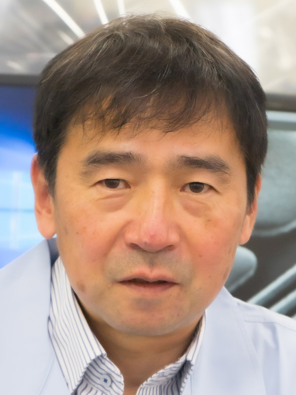 ABSTRACT: As the industry moves toward High Performance Computing (HPC) for huge data transmission with low power consumption. The requirements for PKG structure have become more challenging. The major engineering requirements for HPC application are high-density, high-speed data transmission, low loss, precision manufacturing with low-cost process. High pin count needs large area package with high mechanical stability and low warpage. ABSTRACT: As the industry moves toward High Performance Computing (HPC) for huge data transmission with low power consumption. The requirements for PKG structure have become more challenging. The major engineering requirements for HPC application are high-density, high-speed data transmission, low loss, precision manufacturing with low-cost process. High pin count needs large area package with high mechanical stability and low warpage.
This talk presents the demonstration of Glass Core Substrate with large panel size format. In case of Glass core substrate process, three metallized process were compared process capability, reliability and high-speed transmission characteristics. Filled with Cu method is found out low resistance, high transmission rate and high-power density. In the thermal stress simulation, the heat characteristics and thermal mechanical stress analysis for two types of via shapes, straight and X-shape, were analyzed, which indicated that straight vias were advantageous for suppressing heat generation, while X-shape was for mitigating thermal stress. The reliability test result obtain stable resistance data because of combination of double-sided polymer dielectrics. The double-sided polymer dielectrics owing stress buffer of glass and copper CTE difference. The Filled with Cu method demonstrated with large panel size format max 510x515mm with 6 layers build-up.
Bio: Satoru Kuramochi received the B.E.degrees and M.E.degrees in image science engineering from Chiba University Japan, in 1987 and 1989, respectively. He joined the Research and Development Center, Dai Nippon Printing Corporation, Japan in 1989. He specializes in the fine pattern processes for high density packaging substrate. He holds 51 patents, has published 30 technical papers concerning to high density substrate technologies. He is research fellow in the fine packaging division of DNP.
|
|
Substrate Market Outlook
 E. Jan Vardaman, President and Founder, TechSearch International, Inc. E. Jan Vardaman, President and Founder, TechSearch International, Inc.
ABSTRACT: Substrates are essential for IC packagers. For high performance applications such as AI, server CPU, and network switches build-up substrates with multiple layers are required. Automotive requires substrates that meet special reliability requirements. Many of high-performance packages use a silicon or redistribution layer (RDL) interposer. Regardless of the interposer, silicon or RDL, attachment to a build-up substrate creates the final package. There is also interest in continuing direct chip attach to a high-density organic substrate, with options including a glass core. The ecosystem that suppliers these substrates is primarily made up of companies located outside of North America. Investments in additional capacity and new substrate technology depend on the financial health of this industry.
This presentation provides and analysis of market for substrates with an analysis of the market size based on revenue. An assessment of the health of the industry is provided with an outlook for the future. Geographic location of substrate suppliers is discussed. Supply and demand analysis for build-up substrates is included.
Bio: Jan Vardaman served on the NSF-sponsored World Technology Evaluation Center (WTEC) study team involved in investigating electronics manufacturing in Asia and on the U.S. mission to study manufacturing in China. She is a senior member of IEEE EPS and is an IEEE EPS Distinguished Lecturer. She is a member of SEMI, IMAPS, and SMTA. She received the IMAPS GBC Partnership award in 2012, the Daniel C. Hughes, Jr. Memorial Award in 2018, and the Sidney J. Stein International Award in 2019. She is an IMAPS Fellow. Before founding TechSearch International, she served on the corporate staff of Microelectronics and Computer Technology Corporation (MCC), the electronics industry’s first pre-competitive research consortium.
|
Addressing Advanced Packaging Scaling and Yield Challenges with Mask-less Lithography
![]() Niranjan Khasgiwale, Digital Lithography BU, Applied Materials Niranjan Khasgiwale, Digital Lithography BU, Applied Materials
 ABSTRACT: The AI race is accelerating move towards 3D heterogeneous integrated architectures and density scaling in substrate manufacturing. The extreme power-hungry workloads in data centers necessitates transition to larger chip modules, more build-up layers in substrates and embedding devices to achieve system level performance and power efficiency. The conventional stepper and LDI tools are incapable of meeting layer-to-layer overlay across highly distorted substrates, resulting in yield loss. ABSTRACT: The AI race is accelerating move towards 3D heterogeneous integrated architectures and density scaling in substrate manufacturing. The extreme power-hungry workloads in data centers necessitates transition to larger chip modules, more build-up layers in substrates and embedding devices to achieve system level performance and power efficiency. The conventional stepper and LDI tools are incapable of meeting layer-to-layer overlay across highly distorted substrates, resulting in yield loss.
This talk will cover advances in maskless lithography. The unique approach enables highest resolution at production throughputs while ensuring CD uniformity and overlay accuracy across the entire panel. The digital functions enable wider design and process windows, to shorten time to market.
Bio: Niranjan Khasgiwale heads marketing for the Digital Lithography BU at Applied Materials. He has more than 25 years of experience in the semiconductor equipment industry and joined Applied in 2011 following the acquisition of Varian Semiconductor, where he led strategy and marketing for the implant business unit. He previously held roles with KLA-Tencor and Formfactor. He holds a master’s degree and Ph.D.in Materials Science from Dartmouth College and Lehigh University respectively, and a B.Tech in Metallurgy from the Indian Institute of Technology.
|
|
Addressing New Challenges with Conventional Organic Substrates
 Venkata Mokkapati, Director, Business Development & Application Engineering, AT&S AG Venkata Mokkapati, Director, Business Development & Application Engineering, AT&S AG
ABSTRACT: The industry has been looking for alternative solutions to address substrate challenges, especially integration on larger packages which are even beyond current Jedec standards. There are several technologies that have been proposed which could solve these problems, organic solutions for example. Nevertheless, today these solutions do not come cheap and also with several technical challenges that still has to compete with the advancements in the Silicon world. One of the non-technical challenges being price for both Silicon and Organic solutions, but in different ways. The scope of the talk would be related to these challenges and potential technologies that could address them.
Bio: Venkata Mokkapati is currently Director, Business Development & Application Engineering at AT&S AG based in Austria. Venkata has more than 18 years of experience in the Semiconductor industry and is a certified ICP engineer from Delft University of Technology from where he also holds a PhD. Prior to joining the industry in 2018 as Business Development Manager, Venkata has spent 12 years in academics in various universities/Institutes across Europe and Asia. Venkata also has experience in establishing and running a sole trading company on graphene and other 2D materials. Venkata has authored and co-authored more than 40 peer-review journals/conference proceedings/patents.
|
AInline Metrology System to Continuously Monitor, Quantify, and Report Differences between CAD and Feature Sizes for Every Layer and Step in the Production Process
![]() Dr Robert Bishop, Beltronics Dr Robert Bishop, Beltronics
 ABSTRACT: To produce a new substrate from CAD data, the manufacturer must compensate for both machine-dependent and design-dependent errors. Examples of machine-dependent errors are non-linearities in the lithography lens or direct-write exposure system, which results in resist feature sizes varying as a function of spatial position on the substrate. Examples of design-dependent errors are etching rates that vary as a function of feature size, shape, and metal density in the neighborhood of each feature. Design-dependent errors will be different for each unique patterned layer. A newly developed inline metrology system capable of up to 10 billion measurements in 5 minutes enables errors between CAD data and every feature on the part to be measured in real time and used to produce a revised “Production CAD file” to compensate for these errors. Once the substrate is in production, the same system can be used to continually monitor the process and detect defects in each layer of the substrate relative to the original customer’s supplied CAD data. ABSTRACT: To produce a new substrate from CAD data, the manufacturer must compensate for both machine-dependent and design-dependent errors. Examples of machine-dependent errors are non-linearities in the lithography lens or direct-write exposure system, which results in resist feature sizes varying as a function of spatial position on the substrate. Examples of design-dependent errors are etching rates that vary as a function of feature size, shape, and metal density in the neighborhood of each feature. Design-dependent errors will be different for each unique patterned layer. A newly developed inline metrology system capable of up to 10 billion measurements in 5 minutes enables errors between CAD data and every feature on the part to be measured in real time and used to produce a revised “Production CAD file” to compensate for these errors. Once the substrate is in production, the same system can be used to continually monitor the process and detect defects in each layer of the substrate relative to the original customer’s supplied CAD data.
Bio: Dr. Robert Bishop is the founder of Beltronics Incorporated. He received his doctorate degrees in electronics engineering and computer science with emphasis on neural network systems from MIT and Harvard in 1980. He holds 28 patents across technologies incorporating advances in ophthalmic scanners, OCT, MRI, and CAT scanners, DNA analysis systems, high speed low light image sensors, optics, lasers, digital signal processing technologies, and AI computer algorithms for analysis of complex images.
|
|
Advanced Inspection and Metrology for Glass Panel Processing
 Barton A. Katz, President & Chief Commercial Officer, Nanospan Technologies Barton A. Katz, President & Chief Commercial Officer, Nanospan Technologies
ABSTRACT: Glass Core Panels with dimensions of 510mm x 515mm are of high interest to the industry in terms of advanced packaging applications. Specifically, panel edges have been highlighted as areas of vulnerability relative to cracks and related debris. Based upon existing technology a tool platform has been built that will initially provide inspection of all 4 edges of panels at production speeds. The tool platform encompasses scanning stages in conjunction with up to 7 sensors (probes) that provide a variety of inspection and metrology tasks including panel top edge and side inspection, through-substrate defect detection using infrared analysis for built-up and bonded substrates, and macro inspection capabilities to identify full panel issues. The same technology for inspection has been shown to be effective when performing metrology on through-glass-vias (TGVs) as well as bumps.
Bio: Barton (Bart) Katz is the President & Chief Commercial Officer of Nanospan Technologies. He received his Bachelor of Science in Engineering (B.S.E.) degree in chemical engineering from Arizona State University in 1983. He has been involved in the semiconductor manufacturing and equipment industry for 42 years. He was one of the original founding members of ASML and has been involved in several notable start-up companies in the industry. His latest venture involves the application of unique technologies and techniques in inspection, metrology, and lithography involved in various aspects of semiconductor manufacturing including wafer and panel inspection, substrate-specific inspection such as SiC, glass, and other materials, and metrology related to TGVs and bumps. He’s published numerous articles and papers in leading conferences and publications.
|
Large Form Factor Chiplet Package using an Organic Interposer for Chip-last Assembly
![]() Shingo Hayashibe, Shinko Electric America, Inc. Shingo Hayashibe, Shinko Electric America, Inc.
 ABSTRACT: Interposers that integrate multiple semiconductor chips are rapidly becoming larger. SHINKO’s i-THOP, an organic interposer with 2.3D structure, using semiconductor thin-film technology and Shinko’s assembly processes is one solution for these large size interposers. In this talk, the structure, design, features, and evaluation results of i-THOP will be presented. ABSTRACT: Interposers that integrate multiple semiconductor chips are rapidly becoming larger. SHINKO’s i-THOP, an organic interposer with 2.3D structure, using semiconductor thin-film technology and Shinko’s assembly processes is one solution for these large size interposers. In this talk, the structure, design, features, and evaluation results of i-THOP will be presented.
Bio: Shingo Hayashibe graduated from Shinshu University with BS and MS degrees, then joined Shinko Electric Industries Co., engaged in process development for packaging in the R&D division and plastic substrate packaging technology. Since 2024 he has been at the SHINKO ELECTRIC AMERICA, INC. San Jose office as an Advanced Packaging Specialist.
|
|
Transforming Semiconductor Packaging with Glass-Based Substrates
 Sung Jin Kim, Ph.D., CTO, Absolics Sung Jin Kim, Ph.D., CTO, Absolics
ABSTRACT: The packaging substrate industry is encountering unprecedented challenges driven by the rapid evolution of semiconductor applications, particularly in artificial intelligence (AI), high-performance computing (HPC), and high-frequency radio frequency (RF) systems. As device complexity and performance requirements escalate, addressing critical build-up package substrate challenges is imperative to ensure scalability, efficiency, and reliability. Key challenges encompass interconnect scaling and signal integrity, manufacturability and yield optimization, thermal dissipation, and power delivery. Interconnect scaling and signal integrity are paramount as operating frequencies increase, necessitating high-speed signal transmission while minimizing parasitic losses, crosstalk, and latency. Conventional materials and structures exhibit limitations in dielectric performance, leading to signal degradation at elevated data rates. Researchers are investigating alternative materials and structural innovations, including glass-based packaging, ultra-low-loss dielectric materials, and advanced redistribution layer (RDL) designs. Manufacturability and yield optimization present significant challenges due to the complexity of advanced packaging techniques, requiring stringent process control, advanced metrology, and defect mitigation strategies. As semiconductor packaging transitions toward finer interconnect pitches and denser integration schemes, overcoming these manufacturing hurdles is crucial. Thermal dissipation and power delivery are critical for power-intensive AI and HPC processors. Increasing power densities necessitate highly efficient power delivery networks (PDNs) and innovative cooling mechanisms to prevent thermal-induced performance degradation. Researchers are exploring embedded power delivery architectures, integrated voltage regulation techniques, and advanced cooling structures. The semiconductor industry also contends with supply chain and material challenges. High-performance build-up substrate materials, including glass and advanced organic laminates, require stable supply chains and scalable manufacturing capabilities.
Glass-based build-up substrates hold the potential to enable next-generation electronic systems due to their superior electrical performance, mechanical stability, and scalability. Absolics is at the forefront of pioneering glass-based build-up substrate technologies, redefining electrical, mechanical, and thermal performance benchmarks for advanced semiconductor packaging. The inherent advantages of glass substrates, such as superior signal integrity, dimensional stability, and high-frequency performance, present significant opportunities for enhanced integration and miniaturization. Absolics has secured strategic funding from the U.S. CHIPS Act and the National Advanced Packaging Manufacturing Program (NAPMP) to further explore the application of its glass-based technologies. This presentation systematically explores Absolics’ proprietary glass-based solutions, presenting key technical insights and addressing fundamental industry challenges. Precision glass structuring for high-density device integration, optimized electrical performance and signal integrity, advanced routing efficiency, and supply chain optimization are highlighted as major technological breakthroughs.
By leveraging these advancements, Absolics’ glass-based packaging solutions represent a disruptive innovation in semiconductor packaging, enabling superior performance, scalability, and manufacturability. The topics addressed in this abstract will be comprehensively presented throughout the keynote speech, providing a detailed exploration of the challenges and solutions shaping the future of semiconductor packaging.
Bio: Dr. Sung Jin Kim is the CTO of Absolics, a recently spun-off semiconductor packaging business from SK Group in the USA. With 30 years of experience in the semiconductor and microelectronics packaging industry, Dr. Kim leads new technology and business development for advanced semiconductor packaging solutions at Absolics. Prior to Absolics, he held executive positions in various companies and countries, including SKC, Georgia Institute of Technology, Foxconn Advanced Technology, Daeduck Electronics, UTAC, and Amkor Technology. Throughout his career, Dr. Kim managed package engineering, substrate manufacturing, and embedding component microelectronic package engineering. He has over 100 US patents and holds a doctorate in electrical engineering from the Technical University of Dresden, Germany.
|
Accelerating Advanced IC Substrate Development with Versatile Process Control Solutions
![]() Monita Pau, Onto Innovation Monita Pau, Onto Innovation
 ABSTRACT: Heterogenous integration has been key to address the rapidly growing demand for higher performance and optimal power consumption in advanced end applications like artificial intelligence (AI) and high-performance computing (HPC). Besides the development of various 2.5D and 3D packaging techniques, advanced IC substrate will also need to evolve to support the demand for higher interconnect density. In this presentation, we will explore the manufacturing challenges in these next-generation substrates and discuss the inspection and metrology solutions to support process development and production monitoring. ABSTRACT: Heterogenous integration has been key to address the rapidly growing demand for higher performance and optimal power consumption in advanced end applications like artificial intelligence (AI) and high-performance computing (HPC). Besides the development of various 2.5D and 3D packaging techniques, advanced IC substrate will also need to evolve to support the demand for higher interconnect density. In this presentation, we will explore the manufacturing challenges in these next-generation substrates and discuss the inspection and metrology solutions to support process development and production monitoring.
Bio: Monita Pau is currently Strategic Marketing Director for Advanced Packaging at Onto Innovation. She works with business leaders and executives to drive strategic planning and leads the development of collaborative initiatives to drive growth and innovation. With over 15 years of experience, her expertise spans across frontend and backend of line process control solutions as well as specialty materials for advanced packaging and assembly. Prior to joining Onto, she held various positions in applications engineering, marketing and strategic business development at DuPont and KLA. Monita holds a Ph.D. degree in Chemistry from Stanford University.
|
|
Advanced Packaging Substrate Technologies for Power Efficient AI Products
 Sai Boyapati, Director of Technology Development, AMD Advanced Packaging Sai Boyapati, Director of Technology Development, AMD Advanced Packaging
ABSTRACT: This talk outlines the AMD advancements in power-efficient AI through advanced packaging technologies. It highlights AMD’s end-to-end portfolio, including processors, GPUs, and accelerators designed for various applications from endpoints to cloud computing. Then it discusses the challenges of traditional Moore’s Law scaling, increasing costs, and thermal impacts of silicon scaling. It emphasizes the importance of performance per watt as a critical metric in AI and details AMD’s energy efficiency goals for processors and accelerators. Advanced packaging techniques such as 2.5D and 3D integration are presented as solutions to enhance compute and memory capabilities while addressing power efficiency and thermal management. The presentation also covers AMD’s journey in advanced packaging, future system-in-package architectures, and substrate focus areas for network bandwidth improvement. It concludes with opportunities in advanced packaging, including innovations in materials, substrate processes and architectures.
Bio: Sai Boyapati is a Director of Technology Development in AMD Advanced Packaging organization. He leads an international team of pathfinding and development engineers responsible for defining substrate technology roadmap and enabling building blocks for next generation packages. Over the past 15 years, Sai has authored 52 patents in the areas of substrate materials and architectures to enable breakthrough solutions in interconnect density scaling, power delivery and high-speed IO.
|
The Impact of Policy on Advanced Semiconductors and Packaging Ecosystem for Aerospace and Defense
![]() Timothy Lee, Boeing Timothy Lee, Boeing
 ABSTRACT: The impact of US Government Technology Policies is critical to the funding and timelines to support the development and maturation of advanced semiconductors and packaging ecosystems that support both commercial and aerospace & defense applications. This presentation summarizes the needs & challenges of advanced microelectronics for the warfighter. On-going USG efforts and objectives to on-shore semiconductors and packaging capabilities to provide a more secure supply chain for economic and national security will be discussed. To be successful, domestic capabilities must be supported by demand signals to ensure a sustainable business model. Finally the talk will take a look at most critical need for success – workforce development and what can be done to promote awareness. ABSTRACT: The impact of US Government Technology Policies is critical to the funding and timelines to support the development and maturation of advanced semiconductors and packaging ecosystems that support both commercial and aerospace & defense applications. This presentation summarizes the needs & challenges of advanced microelectronics for the warfighter. On-going USG efforts and objectives to on-shore semiconductors and packaging capabilities to provide a more secure supply chain for economic and national security will be discussed. To be successful, domestic capabilities must be supported by demand signals to ensure a sustainable business model. Finally the talk will take a look at most critical need for success – workforce development and what can be done to promote awareness.
Bio: Timothy Lee is a Boeing Technical Fellow based in Southern California. He leads the development of disruptive microelectronics technologies for advanced communications networks and sensor systems for airborne and space applications. His research interests include 3D Heterogeneous Integration (3DHI) technologies for chiplet/wafer stacking of digital/analog/RF silicon/III-V devices for high-performance, and low-power microelectronics for aerospace and defense application. He is principal investigator for the transition of IRAD, CRAD and university Lab to Fab research into technologies for defense systems. During his over 40 years of experience, he has held technical/managerial positions at research facilities, aerospace companies, and semiconductor foundries. He has led development of hardware for satellite communications and has built phased-array antenna electronics for commercial and US government customers. Lee has authored over 30 journal and conference papers. He leads several Technical Working Groups in the IEEE Heterogenous Integration Roadmap (HIR). He holds SMEE and SBEE degrees from MIT and a master’s degree in system engineering from University of Southern California.
|
|
Small Via Formation in Next Generation IC Substrates
 Jacob Magers, MKS Instruments Inc. Jacob Magers, MKS Instruments Inc.
ABSTRACT: Across a wide field of IC Substrate applications, from Mobile devices to AI Servers, the common themes of increasing complexities, package size, increasing routing densities, smaller lines and spaces, and correspondingly smaller laser drilled vias are prevalent. In addition, material sets are evolving to support high speed data transmission with low loss. This presentation will provide a brief overview of current IC substrate laser via formation technologies using MKS CO2 and UV laser drilling systems and discuss the challenges to be met in next generation IC substrates.
Bio: Jacob Magers is the Applications Engineering Manager for the Geode product group in the Systems Business Unit of MKS Instruments, Inc, based in Beaverton, Oregon. He has worked for MKS in the field of laser-materials processing for 10 years, having joined the company after completing his MS in Applied Physics at the University of Oregon. As an individual contributor, he has been responsible for laser material interactions, process development, laser quality and reliability testing, and beam path design.
|
Equipment Needed for the Build-up Process
![]() Laurent Nicolet, VP of Business Unit Electronics, SCHMID Group Laurent Nicolet, VP of Business Unit Electronics, SCHMID Group
 ABSTRACT: SCHMID Group introduces a modular toolset for advanced IC substrate and HDI+ manufacturing, compatible with both organic and glass cores. The platform supports critical processes such as SAP and Any Layer Embedded Traces (ET), with tool clusters designed for vertical, touch-free, single-panel processing. The Any Layer ET process employs ICP RIE etching and sputtered metallization to replace conventional SAP process, enabling precise, anisotropic features on nonwoven dielectrics like ABF or polyimide. ABSTRACT: SCHMID Group introduces a modular toolset for advanced IC substrate and HDI+ manufacturing, compatible with both organic and glass cores. The platform supports critical processes such as SAP and Any Layer Embedded Traces (ET), with tool clusters designed for vertical, touch-free, single-panel processing. The Any Layer ET process employs ICP RIE etching and sputtered metallization to replace conventional SAP process, enabling precise, anisotropic features on nonwoven dielectrics like ABF or polyimide.
Systems accommodate structures down to 2 µm on panels up to 25″ x 25″, with optimized process control. SCHMID’s cleanroom-based Technology Center offers full prototyping capabilities, bridging R&D and high-volume manufacturing for next-generation substrates. The solution delivers high registration accuracy, material flexibility, and process scalability within ISO6 environments.
Bio: Laurent Nicolet, VP of Business Unit Electronics at SCHMID Group with over 40 years of experience in PCB and substrate manufacturing. He was owner and CTO at CICOR, act as Project Manager at Multek and in 2006, he joins the SCHMID Group and was responsible for the business unit Electronics. In 2009, he was relocated in Asia, Hong Kong and now Taiwan. He specializes in process development and integration for HDI and substrates, with a focus on enabling scalable solutions for both organic and glass core technologies, from R&D to high-volume production.
|
|
Revitalizing Semiconductor Startups: Investment and Innovation Landscape in the CHIPS Act Era
 ABSTRACT: Startups are a critical part of the semiconductor ecosystem, and have been since the birth of the industry, driving growth and innovation in the industry and exploring new frontiers of chip technology. Unfortunately, startups in the semiconductor sector face significant challenges and barriers to entry. The landscape for startups and venture investing will be described in relation to the current investment climate and the CHIPS Act initiatives. ABSTRACT: Startups are a critical part of the semiconductor ecosystem, and have been since the birth of the industry, driving growth and innovation in the industry and exploring new frontiers of chip technology. Unfortunately, startups in the semiconductor sector face significant challenges and barriers to entry. The landscape for startups and venture investing will be described in relation to the current investment climate and the CHIPS Act initiatives.
Bio: Daniel Armbrust is co-founder and director of Silicon Catalyst which incubates semiconductor startups. Its portfolio companies have raised more than $0.8B in venture funding and are valued at nearly $3.0B. Armbrust serves as an advisor, board member, board chairman and angel investor for many semiconductor startups. Daniel is an affiliate with Lawrence Berkeley National Labs and was appointed to the Industrial Advisory Committee, which advises the Department of Commerce on the R&D strategy for the CHIPS Act. He served as President and CEO of the SEMATECH semiconductor consortium and held various positions in semiconductor manufacturing and development over 25 years at IBM.
|
Building a 3D Metropolis of Skyscrapers
![]() Farhang Yazdani, CEO, BroadPak Corporation Farhang Yazdani, CEO, BroadPak Corporation
 ABSTRACT: We present a comprehensive approach to the development of a three-dimensional digital metropolis densely populated with skyscrapers. Leveraging procedural generation techniques, urban planning principles, and architectural modeling, the presentation explores methods for efficiently generating high-rise structures within a cohesive metropolitan layout. ABSTRACT: We present a comprehensive approach to the development of a three-dimensional digital metropolis densely populated with skyscrapers. Leveraging procedural generation techniques, urban planning principles, and architectural modeling, the presentation explores methods for efficiently generating high-rise structures within a cohesive metropolitan layout.
This approach reimagines the package as a vertically structured ecosystem of chiplets and co-packaged optics, akin to a densely built urban skyline while addressing the critical industry challenges in scalability, thermal management, signal and power integrity, and system-level testing by leveraging advanced high bandwidth substrates and stacking technologies. Compute, memory, and I/O functions are modularized into chiplets and interconnected through high-bandwidth, low-latency optical and electrical links, enabling compact, high-performance systems with reduced energy per bit. We present the design principles, enabling technologies, and co-optimization strategies necessary for implementing this architecture in AI, HPC, and data center environments. This work sets a foundation for future computing platforms that demand extreme performance, efficiency, and integration density.
Bio: Farhang Yazdani is the President and CEO of BroadPak Corporation, a provider of advanced 2.5D/3D heterogeneous chiplet integration and co-packaged optics design/manufacturing services based in San Jose, California. Through his 23 years in the industry, he has served in various technical, management, and advisory positions with leading semiconductor companies worldwide. He is the author of the book “Foundations of Heterogeneous Integration: An Industry-Based, 2.5D/3D Pathfinding and Co-Design Approach”. He is the recipient of the 2013 NIPSIA award in recognition of his contribution to the advancement and innovations in packaging technologies. He has numerous publications and IPs related to 2.5D/3D Packaging and Assembly, serves on various technical committees, and is a frequent reviewer for the IEEE Journal of Advanced Packaging. He received his undergraduate and graduate degrees in Chemical Engineering and Mechanical Engineering from the University of Washington, Seattle.
|
|
 ABSTRACT: ABSTRACT:
Bio:
|


 Hikaru Mizuno, JSR Micro
 Shiro Tatsumi, Ajinomoto
 Masa Fukui, Resonac America, Inc.

 Jason Conrad, Chief Operating Officer, ASU Knowledge Enterprise, and Craig Bishop, Chief Technology Officer, Deca Technologies

 Yoshihiro Inoue, Nikko-Materials
 E. Jan Vardaman, President and Founder, TechSearch International, Inc.
 Venkata Mokkapati, Director, Business Development & Application Engineering, AT&S AG
 Barton A. Katz, President & Chief Commercial Officer, Nanospan Technologies
 Sung Jin Kim, Ph.D., CTO, Absolics
 Sai Boyapati, Director of Technology Development, AMD Advanced Packaging
 Jacob Magers, MKS Instruments Inc.