INVITED SPEAKER
FRANCIS BALESTRA, PhD.
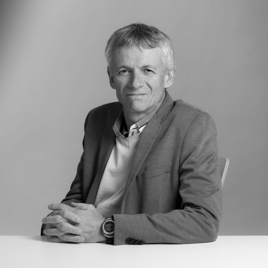
FRANCIS BALESTRA, PhD.
Univ. Grenoble Alpes, CNRS, Grenoble INP, IMEP-LAHC, 38000 Grenoble, France
Sustainable Nanoelectronic Devices for the end of the Roadmap
BIOGRAPHY:
Francis Balestra, Director of Research CNRS, has been Director of several Laboratories. Within FP6, FP7, H2020 and Horizon Europe, he coordinated several European Projects (SiNANO, NANOSIL, NANOFUNCTION, NEREID, ICOS) that have represented unprecedented collaborations in the field of Nanoelectronics. He is member of several European Scientific Councils, of the Advisory Committees of International Journals, of the IRDS International Roadmap Committee, and founded or organized many international Conferences. F. Balestra has coauthored over 500 publications in international scientific Journals, international Conferences, and books or chapters. He is currently Vice-President of Grenoble INP, in charge of European activities, and Director Emeritus of the Europen SiNANO Institute he founded 16 years ago.
For future sustainable societies, a holistic approach is needed with the combination of two pillars: Digitalization of many domains to reduce footprint, Electronic monitoring targeting societal challenges, e.g. energy, health, environment, and Sustainable electronics, including innovative materials, devices, circuits and systems.
The substantial increase of electronic systems and IoT devices, the exponential augmentation of computing power for AI training, the strong growth of ICT share in electrical energy consumption, the problem of E-waste, and the lack of material availability put forward the need of substitution of critical (scarce, toxic) materials, the reduction of energy consumption in electronic systems, and the development of alternative device and system architectures.
This paper presents promising solutions for overcoming these challenges in the areas of nanodevices and nanomaterials, which are at the core of future ICT systems. Nanowires, ultrathin films, gate-all-around structures, advanced materials such as 1D or 2D, alternative device architectures such as steep slope switches, heterostructures, and ultimate nanodevices are highlighted, which will be able to reach the ambitious targets of the IRDS Roadmap for the next decades [1-17].
References
[1] F. Balestra, Nanoscale CMOS: Innovative
Materials, Modeling and Characterization, Francis Balestra Ed., ISTE-Wiley (2010)
[2] F. Balestra, Beyond CMOS Nanodevices (1 & 2), Francis Balestra Ed., ISTE-Wiley (2014)
[3] F. Balestra, Challenges for high performance and very low power operation at the end of the Roadmap, Solid-State Electronics, Volume 155, May 2019, pp. 27-31
[4] F. Balestra, Advanced technologies for future materials and devices, Chapter in Springer Handbook of Semiconductor Devices, to be published, 2022
[5] S.B. Deasy et al, Science, Vol. 354, Issue 6308, pp. 99-102, 2016
[6] W. Chung, IEDM 2017, p. 365 [7] A. Saeidi, IEEE EDL, VOL. 38, No. 10, p.1487, Oct. 2017
[8] M.H. Lee, IEDM 18, p. 735
[9] Z. Yu, IEDM 18, p. 524
[10] A. Saeidi, IEDM 18, p. 304
[11] E.A. Casu., IEDM 16, p. 19.3.1
[12] S. Lim, IEDM 16, p. 34.7.1
[13] C.-H. Yeh et al, DOI: 10.1109/IEDM19573.2019.8993600, IEDM 2019
[14] D. Akinwande et al, doi: 10.1038/s41586-019-1573-9, Nature, Sept. 2019
[15] I. Asselberghs, DOI: 10.1109/IEDM13553.2020.9371926, IEDM 2020
[16] G. Gandus, IEDM 2022
[17] International Roadmap for Devices and Systems, IEEE/IRDS, 202
LORENA GARCIA, MsC.
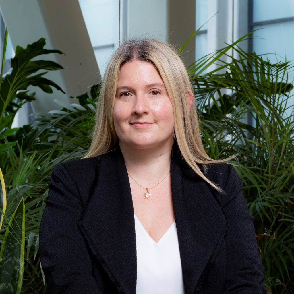
LOREN GARCIA, MsC.
SMIEEE
Assistant Professor, Universidad Central, Colombia
IEEE Educational Activities Board member
IEEE STEM champion
ACIEM Diversity and Inclusion Commission Director
Empowering Innovation: The Impact of the IEEE Foundation
BIOGRAPHY:
Lorena Garcia is a dedicated STEM education leader passionate about advancing diversity and inclusion within the field. With over 16 years of experience in academic and administrative management, teaching, and research, Lorena Garcia holds a Master of Science in Electronic Engineering and currently is an Assistant Professor at Universidad Central in Bogota, Colombia.
Lorena Garcia is a volunteer leader within IEEE and the Colombian Association of Engineers, actively promoting technology and STEM outreach. She holds prestigious positions such as Director of the IEEE Foundation and a member of the IEEE Educational Activities Board (EAB). In 2022, she was honored with the IEEE MGA Leadership Award for her exemplary leadership and impact.
In today’s rapidly evolving technological landscape, organizations like the IEEE Foundation play a crucial role in empowering innovation and advancing engineering solutions for the benefit of society. This presentation will delve into the transformative impact of the IEEE Foundation, highlighting its mission, key initiatives, and the tangible outcomes achieved through its support. We will explore how the Foundation fosters technology and engineering education, nurtures aspiring innovators, and catalyzes research breakthroughs. Through case studies and examples, we will demonstrate how the Foundation’s investments in scholarships, grants, and projects have spurred groundbreaking developments in various fields. Join us to discover how the IEEE Foundation is shaping the future of technology and enabling positive change on a global scale.
JULIANNA M. PICHARDO

JULIANNA M. PICHARDO
Humanitarian Activities & Sustainable Development Manager
IEEE Corporate Activities
USA
BIOGRAPHY:
Julianna Pichardo has a B.A. in Business Administration and Spanish from Messiah College. After college, she worked for over five years at Esperanza International, a microfinance nonprofit dedicated to poverty alleviation in the Dominican Republic. Julianna joined the Humanitarian Technologies team at IEEE in 2018 where she currently supports the Humanitarian Technologies Board’s programs to ensure smooth and consistent processes that lead to meaningful impact.
ALEXANDER KLOES, PhD.
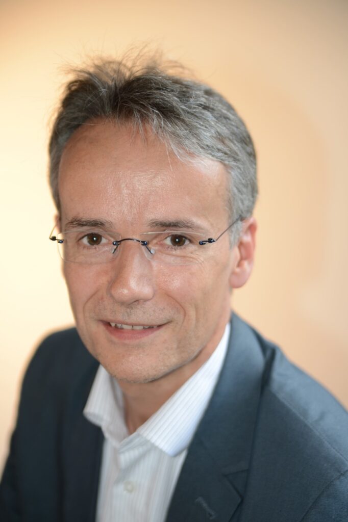
ALEXANDER KLOES, PhD.
THM University of Applied Sciences in Giessen, Germany
Variability-Aware Circuit Design: Monte Carlo Simulation Versus Noise Analysis
BIOGRAPHY:
Alexander Kloes is Professor at THM University of Applied Sciences in Giessen, Germany. He currently serves as Dean of the Department for Electrical Engineering and Information Technology and heads the Device Modeling Research Group at the Competence Center for Nanotechnology and Photonics. In 1996, he received the PhD degree in electrical engineering from Technical University of Darmstadt, Germany. He is IEEE Senior Member, holds 15 patents and co-authored more than 200 research papers. His research interests focus on compact modeling and simulation of semiconductor devices, particularly nanoscale MOS devices and organic thin-film transistors for flexible electronics, and simulation approaches for the design of neuromorphic computing architectures.
For a robust circuit design, from statistical variations of device parameters must be considered. A classical approach is the corner analysis. Worst-case corner models offer designers the capability to simulate the pass/fail results of a typical design and are usually pessimistic. A Monte Carlo (MC) simulation is the standard approach to get more detailed results for the statistical variation of a circuit’s performance depending on given distribution functions for fluctuating device parameters. However, there is a high number of iterations necessary for getting reliable statistical data.
The Noise-Based Variability Approach (NOVA) has been proposed as alternative and numerically very efficient method. It is based on a noise analysis in a circuit simulation with fluctuating parameters of a compact model and allows estimating the statistical variability of state variables in a circuit from only one simulation run.
In this presentation, NOVA is reviewed in comparison to MC simulations for the case of circuits with organic thin-film transistors including parameter fluctuations. Furthermore, results using NOVA for the simulation of the inference process in crossbar arrays of neuromorphic computing structures are shown.
JEEWIKA RANAWEERA , PhD.
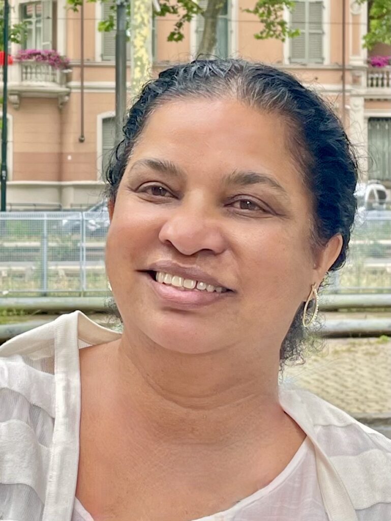
JEEWIKA RANAWEERA, PhD.
Co-Chair Metaverse Initiative of IEEE Future Directions
Bridging Technology and Humanity to Cultivate an Inclusive Metaverse
BIOGRAPHY:
JEEWIKA RANAWEERA is an engineer, author, illustrator, inventor, and sustainability champion. She is an active volunteer for IEEE Future Directions, IEEE Women in Engineering, IEEE Electron Device Society, and IEEE Engineering Accreditation Activities. Her outstanding contributions led to her induction into IEEE-Eta Kappa Nu as a Professional Member of the Eta Chapter of the Board of Governors in 2023. She is a co-chair of the IEEE Metaverse initiative and also a member-at-large for IEEE Women in Engineering.
Jeewika authored an eBook chronicling her engineering journey for IEEE Women in Engineering, aiming to motivate individuals to pursue careers in STEM fields. Additionally, she illustrated the very first children’s book published by IEEE. Recognized as one of the “Women Engineers You Should Know in 2023” by the Society of Women Engineers, she has also been a prominent figure in IEEE WIE Santa Clara Valley, serving as both chair and co-chair. Her dedication earned her the prestigious “Outstanding member who promoted women in engineering” award from IEEE WIE SCV in 2020.
Jeewika is devoted to eliminating bias in artificial intelligence, particularly its discriminatory impact on women and historically marginalized groups. To this end, she initiated a special IEEE Future Directions project aimed at bridging the digital divide and fostering digital equity and inclusion for all. As co-chair of the IEEE Metaverse Initiative, she actively addresses the growing digital divide arising from hardware and connectivity disparities. Her commitment is further demonstrated through her frequent tech talks, wherein she sheds light on these crucial issues.
She attained her bachelor’s degree in computer science and engineering from ISPJAE in Havana, Cuba, followed by her master’s and PhD degrees in Electrical and Computer Engineering from the University of Toronto, Canada. Throughout her academic journey, Jeewika has contributed to numerous technical journal publications and presented her research at international conferences. Her inventive spirit has resulted in the acquisition of five US Patents.
Jeewika Ranaweera’s dynamic skills, unwavering dedication to equality in technology, and numerous accolades serve as an inspiration to aspiring engineers worldwide. Through her pioneering work and tireless efforts, she continues to pave the way towards a more inclusive and innovative technological landscape, benefitting individuals from all walks of life.
In the ever-changing technological landscape, Dr. Jeewika Ranaweera embarks on a journey that intricately weaves together cutting-edge technology, current megatrends, and fundamental human values. This presentation delves into the transformative intersection of the Metaverse and immersive technologies, emphasizing their collective role in shaping a future that eliminates bias in AI. Driven by the aspiration to surpass technological barriers, Dr. Ranaweera aims to foster an inclusive metaverse that not only embraces the latest innovations but also aligns with the megatrends shaping our global landscape. The crucial role of ethical and human-centric design principles becomes apparent as we navigate the complex intersection of technology, megatrends, and humanity. In addition, Dr. Ranaweera will reflect on a metaverse that transcends virtual spaces that simulate real-world chip manufacturing, incorporating 3D models and animations to visualize complex concepts such as semiconductor structures, chip architectures, and manufacturing processes. Join her in envisioning a future where the metaverse seamlessly integrates with prevailing megatrends, creating a harmonious coexistence of innovation and inclusivity. These advancements collectively pave the way for a transformative era, eliminating bias in AI and fostering an equitable and diverse digital realm.
JACOBUS W. SWART , PhD.

JACOBUS W. SWART , PhD.
Professor
FEEC/UNICAMP
Faculty of Elect. & Comp. Eng.
State University of Campinas
IEEE Fellow
Brazil
School 4.0 – Hands on Project Based Learning in STEM and The INCT NAMITEC Network
BIOGRAPHY:
Jacobus W. Swart received his bachelor of Electrical Engineer and Doctor of Engineering degrees in 1975 and 1981, respectively, from the Polytechnic School of the University of São Paulo. After his doctorate, he worked at the following institutions: K. U. Leuven, Belgium, 1982-83, as postdoc.; CTI, Campinas, 1984, as head of Process Engineering; LSI-University of São Paulo, 1985-88, as assistant professor; SID Microelectronics, 1986-1987 as part-time researcher; RTI, USA, 1991, as a Visiting Scientist and since 1988 at the State University of Campinas, as Full Professor until his retirement in 2013, when he assumed the position of collaborator. He served as director of the Semiconductor Components Center from April 1998 to April 2005. From May 2007 to June 2011, he was on leave from the University to serve as Director of CTI Renato Archer. From 2013 to 2019 he worked for imec, Belgium, as a representative in Brazil. He has worked on integration of CCD, nMOS, CMOS and HBT processes, device characterization and modeling, gettering processes, plasma processes, fast thermal processes, silicide formation and characterization, and integrated circuit design. Dr. Swart has published more than 80 articles in International Journals and 200 full-length articles in International Conference Proceedings. He has presented around 150 invited talks and/or tutorials at different conferences, workshops and visits. He supervised 61 postgraduate students, masters and doctors. He is a PQ fellow from CNPq, level 1A and is an Elected Member of the Academy of Sciences of the State of São Paulo and the National Academy of Engineering. He is a Fellow of IEEE, a member of SBMicro, and was president of SBMicro twice, 1988-90 and 1998-2000. He was general coordinator of a large research network in Brazil, called NAMITEC, from 2001 to 2016, which was renewed again from 2022. He is currently Vice-President of SBMicro.
School 4.0 Project was developed at the University of Campinas, UNICAMP, aiming to promote STEM education for pre-university students, focusing primarily on the public education network. The project started with initial support from the University itself and was followed by additional support from Electron Device Society and also from the INCT NAMITEC Network. Two distinct low -cost tools that favor the development of hands-on STEM activities were developed: a) Base board Kit for assembling electronic circuits for introduction to basic electronics, and b) BitDogLab board for teaching programming and carrying out electronic projects involving sensors and actuators These tools are part of an ecosystem of solutions that can be copied, improved, and multiplied at the school level, without any commercial bias.
We run workshops in 10 primary and secondary schools, directly involving 11 teachers and 575 students. Additionally, we conducted a vacation course with students selected by the Campinas Department of Education, benefiting 90 primary school students from the public network. We also participated in the Latinoware congress in Foz de Iguaçu, Brazil (https://latinoware.org), offering two lectures and two workshops on the Base board Kit and BitDogLab. Estimated about 300 people came into contact with the School 4.0 project during Latinoware.
The direct impact of these initiatives was complemented by significant indirect reach, including directors, coordinators, teachers of other disciplines, students, and their families, through social media broadcasts and a Massive Open Online Course (MOOC) from School 4.0 on the Coursera – Unicamp platform, reaching an additional 2,300 participants. These initiatives lay the foundation for future workshops aimed at impacting more than 40,000 young people in Campinas and Itatiba, Brazil. This marks a significant advancement in democratizing access to technological education to a wider audience.
The School 4.0 Project and results will be detailed as the main focus of this presentation. Once it is an important activity in our INCT NAMITEC Network, a brief description of this will also be presented. NAMITEC Network comprises 86 researchers from 17 institutions in Brazil carrying out research on different topics within the field of interest of Electron Device Society. These areas include materials science, semiconductor devices, sensors, applications, and initiatives aimed at societal outreach and education.
Furthermore, this project plays a pivotal role in bridging higher education with secondary and primary education by executing activities in synergy. It integrates the three foundational pillars of education, research, and outreach, which are crucial for sustaining high-quality public education. Through this approach, the project facilitates a seamless connection between different levels of education, promoting a comprehensive educational experience that spans from fundamental to higher education.
M.Sc. JOSE IGNACIO CASTILLO
M.Sc. JOSE IGNACIO CASTILLO
Universidad Autónoma de la Ciudad de México
The Academic Research Production in Iberoamerica: The General and the Engineering Case.
BIOGRAPHY:
He has been working for 27 years in telecommunications and computer industry and academia in 100 national and international projects, as team member or leader on technical and management positions in internet networks, data centers and engineering management. In industry he worked for DICI, IFE, REDUNO-TELMEX and DATACENTER DYNAMICS, being now an independent consultant. In academia he works as a full-time professor-researcher at Autonomous University of Mexico City (UACM) since 2008, directing the Advanced Networking Laboratory; in past he was at UPAEP (99-06) & UTM (98-99). He also worked for BUAP, UAM and UDEFA (Military) Mexico and UPS Ecuador as visiting professor. He wrote 4 books, and 50 journal and conference papers. He has lectured 140 undergraduate & graduate courses. He was an IEEE Computer Society Distinguished Lecturer (2015-2017), till today, he offered 171 keynotes, invited talks and webinars, and 16 tutorials for conferences. He received his bachelor’s degree in sciences degree in Electronic Sciences and his M.Sc. Degree in Electronic Devices, both from the B. Autonomous University of Puebla, Mexico.
We will review the trend in academic publications for Iberoamerican countries, obtaining a ranking in the quantity of publication, then analyzing the contributors to identify changes in trends in the academic research contributions trend in the XXI century, first in general contributions to all areas of knowledge, then for engineering. The general contributions per country include publications, the main areas of knowledge in which each country is centering its talents and resources and the main countries they collaborate with, considering all the areas of knowledge from the SCOPUS database. Iberoamerica could be mapped in 3 groups, the first one includes Spain, Brazil, Mexico, Portugal, Argentina, and Chile, which have produced more than 200,000 documents. The second one includes Colombia, Peru, Ecuador, Uruguay, and Venezuela which have produced between 20,000-200,000 and the third group which includes the rest of the countries producing less than 20,000 documents. In this century some interesting changes in trends have appeared in the general production of knowledge, where Brazil is closer to Spain, Chile overcome Argentina. Even in contributions for engineering Colombia overcomes Argentina and Chile, but also interesting changes among Peru and Ecuador appeared. This curated information will be of high value for researchers and policymakers and leaders for the future development of research contributions by different countries.
RAKESH VAID, PhD.

RAKESH VAID, PhD.
Fulbright Fellow
Fellow IETE, Senior Member IEEE, Member ECS, Life member IAPT
Vice-Chairman – IEEE EDS Delhi Chapter
Professor and Former Head
Department of Electronics,
University of Jammu,
Jammu-180006,(J&K) INDIA
Triboelectric Nanogenerators (TENG) for Future Energy Harvesting Devices
BIOGRAPHY:
Dr. Rakesh Vaid is presently Professor at the Department of Electronics and Director of the Poonch Campus, University of Jammu, Jammu and Kashmir, India. He is a Fulbright Fellow (FNIEAS-2022) at the George Washington University USA; Senior member of IEEE and EDS (USA) and Fellow of IETE (India).
Prof. Vaid has served as: Head, Department of Electronics, University of Jammu (2017-2020); Vice Chairman of IEEE EDS Delhi India chapter (2022-present); Chairman IETE Jammu Centre (2014-2018), Vice Chairman, IETE Jammu centre (2010-12); General secretary- Jammu University teachers association during 2013-14. He was awarded University Gold Medal University of Kashmir-1989 and Young scientist fellowship by J&K Council of Science & Technology in 1999.
Dr. Vaid has more than 100 publications to his credit in national/ international journals and conference proceedings. His area of research include Triboelectric Nanogenerator (TENG); Nano electronics & high k dielectrics; device modelling and simulation; Carbon Nanotubes and Graphene based devices; FinFETs; MOS capacitor & solar cell etc. He has successfully guided 07 Ph.D. and 06 M. Phil students besides 05 students are pursuing their Ph.D. under him. He has successfully completed a major research project sponsored by UGC & SERB, besides completed five medium term projects under Indian nanoelectronics user’s, program (INUP) sponsored by CEN, IIT Bombay.
Dr Vaid has presented his research in various prestigious national/ international conferences with in India and abroad such as MIEL-2006 (Belgrade-Serbia), ICMNT-2006 (Algeria), Nano today 2013 (Singapore), MNE 2014 (Lausanne- Switzerland), 227th ECS meeting 2015 (Chicago-USA), 231st ECS meeting 2017 (New-Orleans, USA), University of Manchester, UK (June 2017), 233rd ECS meeting 2018 (Seattle-USA), IMEC (Leuven-Belgium- September 2019), IEEE MIEL 2019 (Nis-Serbia), 241st ECS meeting 2022 (Vancouver-Canada), University of Tokyo (Japan 2023), LAEDC 2023 (Puebla-Mexico) besides visited many universities such as Stanford, Oxford, Cambridge in USA, UK and Europe.
With to the growing energy requirement and the fast emergence of the Internet of Things (IoT), there is a greater need for the sensors to be used in these IoT systems which is estimated to exceed 200 billion by 2025. Therefore, there is huge requirement for the energy supplies without the recharging and replacement of the charge storage device for their sustainable performance. The triboelectric nanogenerator (TENG) is presently the front runner in this area and has attracted considerable attention due to its high instantaneous output power, broad selection of available materials, eco-friendly and inexpensive fabrication process, and various working modes customized for target applications. The TENG harvests electrical energy from wasted mechanical energy in the ambient environment. Three types of operational modes based on contact-separation, sliding, and freestanding are reviewed for two different configurations with a double-electrode and a single-electrode structure in the TENGs. The output performance and mechanical stability of the flexible TENGs can be affected by two important factors: suitable materials and optimum topologies.
In this presentation, we will demonstrate the fabrication and characterization of low cost, power-efficient triboelectric nanogenerators (TENG) with copper (Cu), Aluminum (Al), gold nanoparticles (AuNPs) as a metal layers and Poly methyl methacrylate (PMMA), poly tetra fluoroethylene (PTFE), Polyimide as a polymer layers. Fluorine tin oxide (FTO) and glass has been used as a non-flexible substrate on which layers were deposited using DC Magnetron sputtering and Spin-Coating technique. These metal-polymer thin layers were then joined together to fabricate different TENG devices using polyurethane (PU) as a spacer. Comparative study of TENGs was conducted using SDS1022-DSO which shows AC sine voltages on pressing and releasing the TENG devices. AC sine voltages of all TENG show different characteristics that are time-varying waveforms. We will present various output performance parameters obtained from all the fabricated TENG devices.
OSAMAH Y. ALHARBI, PhD.
OSAMAH Y. ALHARBI, PhD.
PhD student in Advanced Nano-electronics Lab (Prof. Mario Lanza)
Materials Science and Engineering, PSE
Building 3 (Ibn Sina), Desert side, 2260-WS05
On-chip robust threshold-type resistive switching using two-dimensional materials
BIOGRAPHY:
Osamah Alharbi is a PhD candidate in Materials Science and Engineering at King Abdullah University of Science and Technology (KAUST), Saudi Arabia. He holds a M.Sc. in Materials Science and Engineering from KAUST and a B.Sc. in Electrical Engineering from King Fahd University of Petroleum and Minerals (KFUPM). He is the recipient of the Saudi ministry of education scholarship to study abroad, and the Saudi Aramco scholarship for young engineers. Prior to joining KAUST, he worked as a project engineer in Saudi Aramco for two years, where he was able to save the company a total of 15 million USD. His current research interests focus on advanced nanofabrication and characterization techniques of nano-scale devices with novel 2D materials, integration of 2D materials at the back-end-of-line (BEOL) of CMOS microchips, and SPICE simulations of 2D materials-based devices for neuromorphic computing.
In this talk I will present the first on-chip threshold-type RS devices made of 2D materials. First, we start by fabricating and characterizing 4 µm2 threshold-type RS devices on Si/SiO2 substrates, and we readily achieve high endurances of millions of cycles in multiple devices, and with a low variability of switching voltages and state resistances. Then, we integrate our 2D-materials-based threshold-type RS devices at the back-end-of-line (BEOL) of a silicon microchip containing 180 nm technology-node CMOS transistors – CMOS stands for complementary metal oxide semiconductor; this implies that the active area of the device is 0.05 µm2. When using the same methods and materials used on the Si/SiO2 substrate, we observed a dramatic decrease in the yield and endurance; the reason is the lower number of defects in such small area, which increases the energy-to-breakdown and results in permanent contamination of the 2D material with abundant metallic ones from the electrodes. This teaches all readers a very powerful lesson: whatever works on a SiO2/Si substrate does not necessarily will work on a CMOS microchip. Finally, solved this problem and achieved on-chip forming-free threshold-type RS devices with endurances up to 4 million cycles by engineering the chemical composition of the electrodes on the chip. In particular, we used a novel strategy based on the use of a limited volume of Ag at the interface between the top electrode and the 2D material – too much Ag results in unrecoverable dielectric breakdown and premature device failure.
WILFRIDO MORENO, PhD.
WILFRIDO MORENO, PhD.
.
University of South Florida, Electrical Engineering Dept.
Tampa – Florida
BIOGRAPHY:
Dr. Wilfrido Moreno received his M.S.E.E & Ph.D. degrees in Electrical Engineering from the University of South Florida (USF), Tampa – Florida in 1985 and 1993 respectively. He is currently a Professor in the Electrical Engineering Department at the University of South Florida, Tampa – Florida. Since 1994, Dr. Moreno has been facilitating students and faculty mobility throughout the Latin American region; over 120 faculty members have earned their Doctoral degrees from USF. From 2003 to 2022, Dr. Moreno served as the R&D Initiative Director for the Ibero-American Science & Technology Education Consortium (ISTEC) responsible for fostering Teaching/Learning & Research collaborations throughout the Ibero-american region among ISTEC’s members. Dr. Moreno is a founding member of the former Center for Microelectronics Research, (CMR- 1988), which is currently the Nanotechnology Research & Education Center, (NREC). Dr. Moreno is the author of over 135 technical publications. His research interests are oriented the use of Model Based System Engineering as the basis for systems integration that provide hardware/software solutions to industrial applications in areas such as Digital Signal Processing, Communications, Energy, Robotics, Automation & Control, Nano/Micro-electronics, Medical Engineering and Multimedia solutions applied to engineering education. Dr. Moreno has supervised over sixty master students and twenty five doctoral students.
JUAN MANUEL RAMIREZ-CORTES, PhD.

JUAN MANUEL RAMIREZ-CORTES, PhD.
National Institute of Astrophysics, Optics, and Electronics,
INAOE
Puebla, Mexico
Liquid Content Level Measurement using Optical Interferometry with a p-emf sensor and Neural Networks: A Case-of-Study
BIOGRAPHY:
Juan Manuel Ramirez-Cortes is currently a Professor at the Electronics Department, National Institute of Astrophysics, Optics, and Electronics (INAOE), Mexico, Group of Instrumentation. He received the PhD degree in Electrical Engineering from Texas Tech University in 1992. From 1982 to 2007 he was with University of the Americas, Puebla, Mexico, in several roles as faculty member, Department Chair, Dean of the Engineering School, and Academic Secretary. Since 2007 he has been at INAOE, Puebla, Mexico, where he has served as Electronics Department Chair, Research Director, and currently Titular Researcher. Dr. Ramirez is an appointed member of the Administrative Committee of IEEE Instrumentation and Measurement Society (IMS), and he is currently serving as IMS Society President for the period 2023-2024. He is member of the Mexican National Research System CONACYT, level 2. His research interests include signal and image processing, instrumentation, digital systems, and computational intelligence techniques.
This talk starts with a brief introduction of the IEEE Instrumentation and Measurement Society, field of interest, organization, and current programs. Then, the technical topic is about an experimental case-of-study aiming to provide an approach for indirect measurement of liquid content level using vibration analysis and optical interferometry. The system makes use of a low power He-Ne laser and an optical setup, aiming to sense the vibrations induced when the container is excited with a light wooden stick by a gentle and rapid impact. The sensing element consists of a homodyne adaptive photorefractive detector based on the so-called non-steady-state photo-electromotive force (p-emf) effect. The p-emf sensor transforms the container vibrating pattern into an electric signal which is further processed to obtain the corresponding spectral content. The spectral information is processed with a neural network used as a non-linear function approximator previously trained with data obtained from the system. Evaluation of the system in terms of accuracy and precision is presented through results corresponding to the RMS error and variance obtained on a set of different liquids.
CRISTIÁN ELIECER BELLO REYES

CRISTIÁN ELIECER BELLO REYES
Quantum Computing Research Group
Physics Department
National University of Colombia
Phase estimation and error mitigation in superconducting quantum processors
BIOGRAPHY:
Cristian E. Bello, a mathematics student at the National University of Colombia, is co-founder and current director of the largest quantum computing research group in the country. In addition, he has played prominent roles as a researcher at the Center of Excellence in Artificial Intelligence and Quantum Computing. His research areas focus on three fundamental areas: Artificial Intelligence (AI), High Performance Computing (HPC) and Quantum Computing (QC). Cristian has distinguished himself in numerous prestigious international conferences and has been distinguished with invitations to present his work at the Abdus Salam International Center for Theoretical Physics (ICTP) in Italy. Beyond his academic work, Cristian is committed to science outreach as a means to overcome the historical barriers that limit access to quality education in Latin America
Quantum phase estimation (QPE) is a key quantum algorithm for performing chemical and solid-state computations in fault-tolerant quantum computers. Recently, several authors have proposed alternatives to QPE that have advantages in early fault-tolerant devices, including shorter circuits and better suitability for error mitigation techniques. However, practical implementations of the algorithm on real quantum processors are lacking. In this work, we implemented phase estimation in superconducting processors. Specifically, we use the quantum Fourier transform to reduce the circuit depth. We use bit-flip bit-read error mitigation strategies. We propose a simple method for estimating energies from phase estimation data, which improves the accuracy of the final energy estimates by one to two orders of magnitude over previous theoretical limits, reducing the cost of performing accurate phase estimation calculations. Our work demonstrates that the estimation has a natural resistance to noise, especially after mitigating coherent errors, and can achieve much higher accuracy than previous methods suggested, demonstrating its potential as a valuable quantum algorithm for early fault-tolerant devices
FABIAN M. BUFLER, PhD.
FABIAN M. BUFLER, PhD.
IMEC
Bélgica
Temperature Dependence of Quasi-Ballistic Transport in n-Type and p-Type Nanosheets
BIOGRAPHY:
Fabian M. Bufler received the Dipl.-Phys. degree in physics from the RWTH Aachen in 1992, the Dr.-Ing. degree in electrical engineering from the University of Bremen in 1997 with a thesis on Monte Carlo simulation of transport in SiliconGermanium, and the venia legendi from ETH Zurich in 2003 with a habilitation thesis on Monte Carlo device simulation of strained-silicon MOSFETs, respectively.
From 2004 to 2017 he was with Synopsys Switzerland LLC (until the take-over in November 2004 Integrated Systems Engineering ISE AG) where he developed the Sentaurus Device Monte Carlo simulator and worked on TCAD applications for advanced CMOS technologies.
He joined the TCAD team of IMEC in Leuven as a senior R&D engineer in 2017 where his main focus is on advanced devices for future technology nodes.
Dr. Bufler has been giving lectures at ETH Zurich on transport theory and Monte Carlo simulation from 2000 to 2020 and has authored or co-authored more than 70 journal articles and peer-reviewed conference proceedings papers.
In 2004 he had an invited talk at IEDM and his h-index is 14. He has served on the program committee of the Electrochemical Society Meeting (SiGe and Ge) in 2006 and 2008 and has been a program committee member of the ESSDERC conference from 2016 to 2023.
The performance of nanosheets with a gate length of 14 nm is investigated by Monte Carlo (MC) and drift-diffusion (DD) simulation between 77 K and 400 K. Increasing at fixed workfunction the temperature from 300 K to 400 K leads for MC to an on-current (ION) increase as opposed to a reduction in DD.
This is related to the quasi-ballistic regime which involves little phonon scattering reducing the temperature-induced penalty in contrast to a strong phonon-limited mobility
degradation in DD. The same physics yields below 300 K to a stronger ION improvement for DD than for MC.
In addition, the subthreshold swing is below 300 K for MC substantially worse than for DD.
These results will have a strong impact on the thermal limitations of chip operation and the viability of cold CMOS.
JOSE LUIS URIBE, MsC.

JOSÉ LUIS URIBE, MsC.
HPE Aruba R&D
Costa Rica
HPE Costa Rica R&D: Creating solutions at worldwide level
BIOGRAPHY:
José Luis Uribe has worked in the networking world for the last 12 years in different roles and positions in research and development, network design, and sales strategy at Hewlett Packard Enterprise. He has been a developer and verification engineer of integrated circuits for networking devices, an account manager for large companies in Colombia, and is currently a Senior R&D manager in Costa Rica. He is Electronics Engineer and Systems Engineer from Pontificia Universidad Javeriana (Bogota, Colombia) and a Master’s degree in Computer Science and MBA from Universidad de los Andes (Bogota, Colombia)
In the Research & Development Center of Hewlett Packard Enterprise in Costa Rica, we have an entire R&D value chain for the invention, design, and development of switching networking devices that are deployed and used worldwide in several verticals and by millions of users. We started 15 years ago, and we want to show you our most important outcomes and how our team has grown based on the Costa Rica talent. We think it may be a data point for more industries and enterprises to expand their R&D operations in the Latin America region in the coming years.