INVITED SPEAKER
ALEXANDER KLOES, PhD.
ALEXANDER KLOES, PhD.
Professor at THM University of Applied Sciences in Giessen, Germany
Critical Evaluation of Methods for Statistical Circuit Simulation Considering a Bias-Dependent Device Variability
BIOGRAPHY:
Alexander Kloes is Professor at THM University of Applied Sciences in Giessen, Germany. He currently serves as Dean of the Department for Electrical Engineering and Information Technology and heads the Device Modeling Research Group at the Competence Center for Nanotechnology and Photonics. In 1996, he received the PhD degree in electrical engineering from Technical University of Darmstadt, Germany. He is IEEE Senior Member, holds 15 patents and co-authored more than 200 research papers. His research interests focus on compact modeling and simulation of semiconductor devices, particularly nanoscale MOS devices and organic thin-film transistors for flexible electronics, and simulation approaches for the design of neuromorphic computing architectures.
For obtaining a high yield in the fabrication of microelectronic systems device variability must be considered in circuit design. We review classical approaches like Monte Carlo simulation and a noise-based simulation technique for the example of an organic thin-film transistor technology. We show that both methods lack from the definition of statistically independent model parameters and can overestimate the drain current variability of a single device. In comparison, a physics-based model for the drain-current variability provides more accurate results in comparison to measurements, but this approach is usually limited to a corner analysis regarding global process variability. In order to introduce this model to mismatch analysis in a numerically efficient way, we propose an improved noise-based approach from the perspective of circuit simulation in a standard EDA tools and demonstrate its benefits with a mismatch analysis of a current mirror.
ANTONIO J. GARCIA LOUREIRO, PhD.
ANTONIO J. GARCIA LOUREIRO, PhD.
Associate Professor at Universidad de Santiago de Compostela
Optical Power Converters based on SiC for space applications: the RePowerSiC initiative
BIOGRAPHY:
Antonio J. Garcia Loureiro received an MSc in Electronic Physics and a PhD in Electronics and Computer Science from the University of Santiago de Compostela (Spain) in 1994 and 1999, respectively. He is currently a professor in the Department of Electronics at the same university. He has also been a visiting researcher at the Edinburgh Parallel Computing Centre (EPCC), UK, and the Device Modeling Group at the University of Glasgow, UK.
His current research interests include the development of numerical simulators for advanced semiconductor devices, solar cells, and power converters. He has published over 100 papers in high-impact peer-reviewed journals, with more than half co-authored with international collaborators, and has presented at more than 150 international conferences. Over the past ten years, he has served as principal investigator on several national and international research projects. He is also the coordinator of the EU Pathfinder Project, RePowerSiC. Additionally, he has supervised 15 PhD theses in this field.
Optical Power Converters based on SiC for space applications: the RePowerSiC initiative
High-power laser transmission (HPLT) stands out as one of the most promising forms of wireless power transfer, thanks to its capacity to transmit energy efficiently across distances—unlocking a wide range of emerging applications. This technique utilizes monochromatic laser light to deliver energy to distant systems through a optical power converter (OPC). Currently, Gallium Arsenide (GaAs) OPCs lead in efficiency, achieving around 69% at light intensities of approximately 11 W/cm². However, their performance significantly drops at higher intensities due to inherent series resistance losses, which stem from their relatively low bandgap energy.
The RePowerSiC initiative, https://repowersic.eu/, aims to overcome these limitations by designing a next-generation, high-efficiency laser power converter optimized for intensities near 1 kW/cm², marking a significant leap forward in HPLT capabilities. The project follows two approaches: first, incorporating advanced materials with higher bandgap energies, and second, introducing cutting-edge OPC architectures. At the core of RePowerSiC are silicon carbide (SiC) polytypes with bandgap energies exceeding 2.3 eV, which is over 50% greater than GaAs, along with novel device designs that target series resistances around 10⁻⁴ Ohm·cm²—more than ten times lower than those in GaAs-based devices.
The project’s ambitions include achieving conversion efficiencies greater than 80%, enhancing power transfer density by more than an order of magnitude over current technologies, and developing eco-friendly, cost-effective manufacturing methods. RePowerSiC promises scalable solutions capable of transmitting kilowatt-level power, enabling smaller OPC footprints and potentially eliminating the need for onboard batteries.
This groundbreaking and high-impact technology could transform power delivery to remote systems, offering exciting possibilities for space-based applications such as satellites, rovers, landers, and in-orbit power distribution. Moreover, it paves the way for innovative use of SiC materials and opens new frontiers in energy transmission and system design.
EDGARDO SAUCEDO, PhD.
EDGARDO SAUCEDO, PhD.
Photovoltaic Group, Electronic Engineering Department
Polytechnic University of Catalonia (UPC) – BarcelonaTech
Emerging inorganic thin film materials for innovative photovoltaic applications
BIOGRAPHY:
Prof. Dr. Edgardo Saucedo received his PhD in Materials Physic at the Universidad Autónoma de Madrid in 2007. In 2007, he joined the IRDEP (Paris, France), working in the development and optoelectronic characterization of CIGS low cost based solar cells. From 2010-2020 he was the Deputy Head of the SEMS Group at IREC working in emerging thin film photovoltaic materials. In 2020 he becomes Professor at the Polytechnic University of Catalonia (UPC).
He holds 6 patents and has co-authored more than 270 papers and more than 400 contributions to International Conferences. He has been involved in more than 40 European and Spanish Projects, and he was the Coordinator of the ITN network Kestcell, the RIA project STARCELL, and the RISE project INFINITE-CELL for the development of Kesterites. In 2019 he was granted with an ERC-Consolidator (SENSATE), for the development of low dimensional materials for solar harvesting applications.
He has supervised 17 PhD Thesis and is currently supervising 8 more. He has an h factor of 52 and more than 9000 citations. In 2020 he has been awarded with the ASEVA-Toyota Award for his contribution to the development of sustainable photovoltaic technologies using vacuum techniques, and ICREA Academia Award in 2021.
Emerging inorganic thin film materials for innovative photovoltaic applications
Edgardo Saucedoa,b
a Universitat Politècnica de Catalunya (UPC), EEBE, Av. Eduard Maristany 10-14, Barcelona 08019, Catalonia, Spain.
b Universitat Politècnica de Catalunya (UPC), Barcelona Centre for Multiscale Science & Engineering, Av. Eduard Maristany 10-14, Barcelona 08019, Catalonia, Spain
There is an increasing interest in the development of novel thin film photovoltaic absorbers with exotic properties for advanced photovoltaic applications, including flexible devices, indoor photovoltaic energy generation, semitransparent/transparent and tandem solar cells. Among them, inorganic chalcogenides and chalco-halides are attracting a lot of attention thanks to their tunability in terms of physical/chemical properties, versatility in terms of synthesis/deposition methods and devices configuration, excellent stability, and competitive performance.
This presentation will show an overview of the latest developments achieved in the Emerging Thin Film Photovoltaic Laboratory at the Polytechnic University of Catalonia (Barcelona, Spain), in the synthesis and photovoltaic application of emerging chalcogenide and chalco-halide materials. The presentation will start with the most recent progresses on kesterite (Cu2ZnSn(S,Se)4) solar cells, with a detailed description of molecular inks route, and the strategies to be followed to achieve conversion efficiencies at the 15% level. Then, emerging van der Waals materials will be introduced, including the synthesis of Sb2Se3 and novel chalcogenides based on the system (Sb,Bi)(S,Se)(Br,I). The development of a high-pressure annealing method for the synthesis of this family of materials will be presented, and the most relevant physical/chemical properties as well as first devices will be shown and discussed.
Following, key developments on semi-transparent Selenium based solar cells will be presented, showing the pathways to fabricate efficient devices by using evaporation techniques. The presentation will finish with a personal point of view of the future of inorganic thin film photovoltaic materials for energy applications.
FRANCISCO GAMIZ, PhD.

FRANCISCO GAMIZ, PhD.
Laboratory of Nanoelectronics.
Research Center for Information and Communication Technologies. CITIC-UGR
Universidad de Granada
Two-dimensional materials in More than Moore Electronics.
BIOGRAPHY:
Prof. Francisco Gamiz graduated with honors in Physics (National Award, Spanish Ministry of Education) in 1991 and obtained his Ph.D. (Extraordinary Award) in 1994 at the University of Granada (UGR). His research began with Monte Carlo simulations of semiconductor devices, leading to international collaborations with institutions like the TJ Watson Research Center of IBM (1999), TU Wien (2000, 2002) and Glasgow University (2006) or Grenoble INP (2008).
Prof. Gamiz has played a pivotal role in several European research projects. He coordinated the EUROSOI and EUROSOI+ projects under EU FP6 and FP7, which established the EUROSOI conference series on SOI technology, today EUROSOI-ULIS conference. As a member of the Governing Board of the SINANO Institute, he has contributed to advancing European Nanoelectronics. Since 2010, he has secured over €10M in funding from the Spanish Government, establishing the Laboratory of Nanoelectronics, Graphene, and 2D Materials at CITIC-UGR.
He has collaborated with leading organizations, including SOITEC, Imec, CEA-Leti, STMicroelectronics, and GlobalFoundries, and participated in major EU industrial projects such as REACHING-22, Place-2B, WAYTOGOFAST and REMINDER. Currently, he is Head of the +QCHIP University Chair under Spanish Chip Law, and advisor for several EU Marie Curie grants. Prof. Gamiz is also a member of the Science Academy of Granada, driving innovation in semiconductor and nanoelectronics research.
Two-dimensional materials (2DMs), such as graphene, have captivated the scientific and engineering communities with their exceptional electronic, optical, and sensing properties. Yet, despite over 15 years of breakthroughs, their industrial integration remains limited—hindered by the dominance of mature silicon technologies and persistent fabrication challenges, including doping, etching, dielectric deposition, and contact engineering.
This talk explores the path forward by focusing on the co-integration of 2DMs with silicon CMOS platforms at both the front-end and back-end of the line. This strategy opens new horizons for high-performance, low-footprint applications beyond conventional silicon, particularly in photonics, biosensing, and flexible electronics.
We highlight ongoing international efforts at the University of Granada that leverage 2DMs in developing scalable, cost-effective graphene-based biosensors, gas detectors, and integrated optoelectronic systems. These projects aim to address real-world demands in healthcare, environmental monitoring, and next-generation computing, showcasing how 2DMs can drive More-than-Moore innovation. The presentation will outline both the remaining hurdles and the exciting opportunities that position 2DMs as enablers of the post-CMOS era.
MARIO LANZA, PhD.
MARIO LANZA, PhD.
Associate Professor of Materials Science and Engineering National University of Singapore
BIOGRAPHY:
Dr. Mario Lanza is an Associate Professor of Materials Science and Engineering at the National University of Singapore, since August 2024. He got the PhD in Electronic Engineering in 2010 at the Autonomous University of Barcelona, where he won the extraordinary PhD prize. In 2010-2011 he was NSFC postdoctoral fellow at Peking University, and in 2012-2013 he was Marie Curie postdoctoral fellow at Stanford University. In September 2013 he joined Soochow University (in China), where he promoted until the rank of Full Professor. Between October 2020 and July 2024, he was full-time Associate Professor at the King Abdullah University of Science and Technology (in Saudi Arabia), where he became known for his work in the field of nano-electronics. He has published over 200 research articles in top journals like Nature, Science and Nature Electronics, many of them becoming highly cited. He has been plenary, keynote, tutorial, and invited speaker in over 150 conferences, and he and his students have received some of the most prestigious awards in the world (like the IEEE Fellow). He has been often consulted by leading semiconductor companies and publishers. He is an active member of the board governors of the IEEE – Electron Devices Society and has been involved in the technical and management committee of top conferences in the field of electron devices, including IEDM, IRPS and IPFA. He speaks fluently five languages: English, Chinese, German, Spanish and Catalan.
WALTER M. WEBER, PhD.
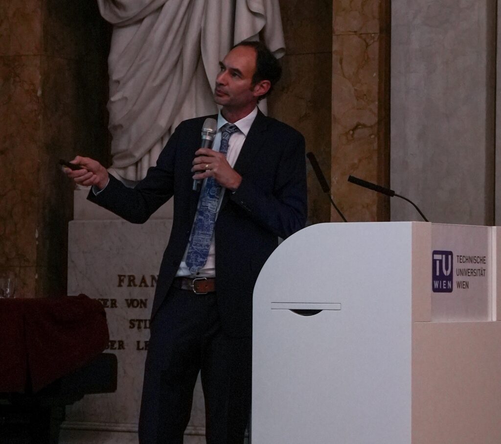
WALTER M. WEBER, PhD.
Professor of Nanoelectronics
Technische Unversität Wien, Vienna, Austria
Silicon-Germanium and Germanium nano-sheet FETs: from reconfigurable functionality to ferroelectrically enhanced neuromorphic operability
BIOGRAPHY:
Walter M. Weber studied Electrical Engineering at TU Munich, Germany, where he graduated as Dipl.-Ing. (MSc equivalent) in 2004 and as PhD in 2008.
Dr. Weber is Professor of Nanoelectronics at TU Wien, director of the Institute of Solid State Electronics and head of the Center of Micro- and Nanostructures – ZMNS-, the central clean room facilities of TU Wien in Vienna Austria. He is an internationally renowned expert in the fields of novel semiconductor devices for logic, memory, sensing and neuromorphic applications, as well as semiconductor technology. He has authored and co-authored more than 180 peer-reviewed scientific papers. Prof. Weber is strongly involved in teaching in the fields of semiconductor-devices and -technology.
Born and raised in Mexico City, the scientific career of Walter Weber began in industrial semiconductor research, 2002-2006 at Infineon Technologies AG – Corporate Research Department and later (2006-2008) at Qimonda AG – Materials Research Department, both in Munich, Germany. There he contributed to the technological development of novel nanometer-scale SOI, finFET and nanowire transistors for logic and multi-bit memory and conceived the concept of reconfigurable transistors. From 2008 to 2019 he acted as Senior Scientist at the Nanoelectronic Materials Laboratory – Namlab gGmbH – in Dresden, Germany, where he was responsible of setting-up and coordinating the clean room and semiconductor technology. In addition, he led the “Emerging Devices“-group dedicated to the development of novel transistors and sensors, material screening for memories. In winter 2010/11 he was visiting Scientist through the Korean Excellence Program at POSTECH University in Pohang, South-Korea. From 2012 to 2019 he acted as a Research Group Leader at the Cluster of Excellence “Center for Advancing Electronics Dresden, CfAED” at TU Dresden, advancing reconfigurable electronics up to the level of circuit enablement, electronic design automation and transfer to industry. In 2019 W. M. Weber was appointed as full professor of Nanoelectronics at the Faculty of Electrical Engineering and Information Technology at TU Wien in Vienna, Austria. His current research is the development of nanoelectronic device concepts for energy-efficient and adaptable Beyond CMOS applications, quantum electronics and sensors as well as the design of dedicated devices for neuromorphic applications.
In this presentation I will focus on an emerging type of semiconductor device family based on ultrathin sheets and nanowires of Si, SixGe1-x and Ge which are epitaxially grown on SOI substrates and contacted by single crystal Al contacts. The device platform allows for four distinct Beyond CMOS device realizations.[1-3] Thus, the transistors composed of an intrinsic and electrically isolated channel can be used to provide a) runtime reconfigurable charge polarity control (RFETs), b) negative differential resistance (NDR-FETs) at room temperature, c) ferroelectric gating for non-volatile memory as well as charge carrier control and finally (FeRFETs) d) Josephson Ge FETs (JoFETs) operability at dilution-cryogenic temperatures [10].
For fabrication, epitaxial growth of SixGe1-x and Ge layers on (100) oriented SOI via ultra-low-temperature MBE, and Mesa structuring. Junction formation is realized via an Al exchange reaction [4], where Al replaces the outdiffused Si and Ge atoms, delivering flat and abrupt single-crystalline and single-elementary Al /semiconductor junctions. Independent gate electrodes are patterned at the Schottky junctions and within the channel.
Reconfigurable field-effect transistors (RFETs) are a novel device concept that fuse n- and p-FET transport properties in a single universal transistor type, as determined by the application of a voltage at the Schottky junctions. [6-7] Thereby, overruling the limitations of rigid conventional CMOS [2]. Runtime reconfiguration can be used at a fine grain manner to build generic circuits that define their actual circuit topology by the applied programming signals. Thereto, novel circuit concepts for adaptive computing and logic gates with reduced transistor count and latencies can be thus designed. Especially minority (MIN), majority (MAJ) or XOR/XNOR based logic benefit from the symmetrical fine-grain reconfigurability, as their implementation in conventional CMOS technology is of higher complexity [7]. Thereto it has been recently possible to demonstrate a reconfigurable single bit-adder making use of only eight identical RFETs. Moreover, the reconfigurability at the device level has been identified as primitives for hardware security circuits.
Negative Differential Resistance (NDR) can be retrieved by integrating pure Ge channels in RFETS being able to operate even above 300K. [8] The mechanism is attributed to the electron transferred effect from the low-effective-mass L valley to the higher effective-mass X valley. By applying channel gating, the NDR region can be entered and the peak to valley ratio can be tuned allowing for circuit reconfigurability at runtime. Our devices can be further equipped with Hf0.5Zr0.5O2, as ferroelectric gating material. Non-volatile programming is realized, remanent polarization adjacent to the Schottky junctions. Apart from non-volatile programming of p- and n-type transfer characteristics the progressive tuning of PG allows for adjustment of the charge carrier tunneling at the Schottky junctions and thus setting of intermediate current states in both and thus reversible directions [9].
HARRI LIPSANEN, PhD.

HARRI LIPSANEN, PhD.
Head of Nanoscience and Advanced Materials Group
Department of Electronics and Nanoengineering
Micronova Research Centre
Aalto University
Broadband miniaturized spectrometers with van der Waals junctions
BIOGRAPHY:
Prof. Harri Lipsanen received his PhD from Helsinki University of Technology in 1994. Since 1999 he has been a Professor of Nanotechnology in Aalto University, Finland. He has held several positions as Head of Laboratory and Department during past 20 years. In 2018 he was Nokia Foundation Visiting Professor in the University of Arizona, USA. He studies nanomaterials and nanofabrication for various applications in photonics and nanoelectronics. His current research focus on materials includes graphene and other 2D materials, compound semiconductor nanowires and their heterostructures. Prof. Lipsanen has co-authored over 450 peer-reviewed articles.
Broadband miniaturized spectrometers with van der Waals junctions
Miniaturized spectrometers are crucial for applications in on-chip and implantable devices, requiring high spectral resolution in limited spaces. Here, we present our van der Waals heterojunction-based spectrometers that achieve tunable spectral responses through band structure engineering, offering sub-nanometer wavelength resolution and a broad operational bandwidth of ~500 to 1600 nanometers.
ANGÈLE REINDERS, PhD.

ANGÈLE REINDERS, PhD.
Professor of Design of Sustainable Energy Systems
Energy Technology & Fluid Dynamics
Department of Mechanical Engineering
Eindhoven University of Technology
The Netherlands
Luminescent solar concentrator photovoltaics: design and simulations of new types of applications
BIOGRAPHY:
Angèle Reinders is a full professor of ‘Design of Sustainable Energy Systems’ at the Department of Mechanical Engineering in Eindhoven University of Technology. She aims at an optimal use and integration of sustainable energy technologies in products, buildings and local infrastructures. In this design-driven research theme improved designs of sustainable energy systems are explored and also developed by means of simulation, prototyping and testing. A strong interest exists in optimized applications of solar energy technologies in the context of buildings and mobility and affiliated energy technologies that support storage, enhanced user interactions and flexibility of sustainable energy.
My aim is to enhance design-driven research on sustainable energy products and systems to support the energy transition
ACADEMIC BACKGROUND
Angèle Reinders studied experimental physics at Utrecht University, where she also received her doctoral degree in chemistry. At present her research has a design-driven scope and as such it is trans-disciplinary, with a focus on performance of energy technologies, environmental aspects, user interactions as well as prototyping and testing of innovative energy products.
Angèle Reinders was the Director of Solliance (2023-2024), and an Associate Professor at University of Twente (2002-2023). From 2010 to 2017 she was appointed as a full professor of Energy Efficient Design at the Faculty of Industrial Design Engineering in TU Delft. In the past she conducted research at – among others – Fraunhofer Institute of Solar Energy in Freiburg, the World Bank (2000) in Washington, D.C., ENEA (2010) in Naples, Center of Urban Energy (2013-2014) in Toronto and in the remote areas of Papua in Indonesia. Also she was a visiting professor at the School of Photovoltaics & Renewable Energy Engineering of UNSW in Sydney (2019-2023).
She is known for her books at Wiley’s “The Power of Design” (2012) and “Photovoltaic Solar Energy From Fundamentals to Applications” (Volume 1 in 2017, Volume 2 in 2024) and her involvement in the IEEE PVSC conference which she chaired in 2014 and 2017. In 2010 she co-founded the Journal of Photovoltaics for which she serves as an editor. In 2014 she received the PVSC Napkin Award in the USA for her contributions to the field of solar photovoltaics. Also she is involved in various tasks of the International Energy Agency PVPS program among which Task 17 on PV for Transport and Task 1 on Strategic PV Analysis & Outreach.
Projects which she has been leading range from design-driven research projects on solar powered mobility to applied PV research at Solliance to exclusively research-oriented projects like her ongoing work on Luminescent Solar Concentrator Photovoltaics (LSC PV), COST Action PEARL PV, https://www.pearlpv-cost.eu/, and ERA-Net Smart Grid Plus Project CESEPS, http://ceseps.nl/.
Luminescent solar concentrator photovoltaics: design and simulations of new types of applications
This presentation will focus on opportunities and challenges of luminescent solar concentrator photovoltaic (LSC-PV) technology in the context of the design of new types of LSC PV applications. The focus of this presentation is on ray-tracing simulations of various LSC PV applications with different geometries for optical and electrical optimization.
An LSC PV is a technology for harvesting solar energy that consist of PV cells attached to a transparent, thin, shaped plate acting as a concentrating lightguide. This luminescent solar concentrator (LSC) contains luminescent pigments, usually called ‘dyes’, that cause, among others, a red shift (up-conversion) of the incoming irradiance spectrum which better matches the wavelength-dependent efficiency of silicon solar cells or other PV technologies. These PV cells are attached to the edges or back of the LSC. This technology needs to be optimized for built-environment conditions, regarding its geometrical design, optical properties, coloring, temperatures, durability and system integration.
It is shown that the typical material properties of LSCs—low cost, colorful, bendable, and transparency—offer a lot of design freedom. Moreover, it is shown that the efficiency of an LSC PV device can exceed the assumed maximum efficiency of 10%, namely close to 19%, which seems a competitive value as compared to other PV technologies in the present market. This presentation is illustrated by visual examples resulting from conceptual design studies.
TRUPTI RANJAN LENKA, PhD.
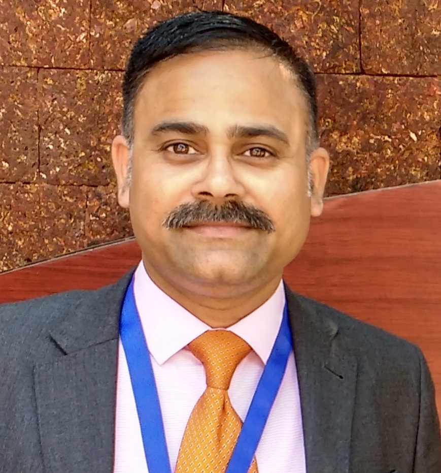
TRUPTI RANJAN LENKA, PhD.
Postdoctoral Researcher
Department of Electrical and Computer Engineering
Texas Tech University, Lubbock, TX, USA
—
Associate Professor
Dept. of Electronics & Communication Engineering
National Institute of Technology Silchar, Assam, 788010, INDIA
(An Institution of National Importance by MoE, Govt. of India)
BIOGRAPHY:
- Dr. Trupti Ranjan Lenka is currently pursuing Postdoctoral Research in the Department of Electrical and Computer Engineering at Texas Tech University, Lubbock, Tx, USA since Dec 2024. He is the Associate Professor of Electronics and Communication Engineering at National Institute of Technology Silchar, Assam, India. He has more than 20 years of experience in academic and electron device research. He received Ph.D. degree in Microelectronics Engineering from Sambalpur University, India in 2012, M. Tech degree in VLSI Design from Dr. A. P. J. Abdul Kalam Technical University, Lucknow, India in 2007 and B.E. degree in Electronics and Communication Engineering from Berhampur University, India in 2000. He was a Visiting Researcher to New Jersey Institute of Technology, Newark, USA in 2019 and Solar Energy Research Institute of Singapore, NUS Singapore in 2018. He visited several countries to present his research at IEEE International Conferences.
- He received the 2023 Outstanding Researcher Award, 2023 Best Researcher Award, 2021 Outstanding Volunteer Award by IEEE Kolkata Section, 2021 IEEE EDS Student Branch Chapter of the Year Award, 2021 Distinguished Researcher Award, 2019 Distinguished Faculty Award and 2018 Visvesvaraya Young Faculty Research Fellowship Award by the MeitY, Govt. of India. He has been awarded as Solar Chartered Engineer by SESI, Certified Professional Engineer and Chartered Engineer by IEI. He is a Fellow of IETE and Fellow of IEI; Senior Member of IEEE; Member of IET, OPTICA, SPIE, IOP, SSI; and Life Member of ISTE, OBA and OPS.
- He is an elected member of the Board of Governors (BoG) of IEEE EDS (2025-2027) and currently engaged in EDS Technical Committee Member of Optoelectronics Devices Committee; Compound Semiconductor Devices and Circuits Committee; Photovoltaic Devices Committee; and EDS Membership and Services Committee. He has been the founder of IEEE EDS NIT Silchar Student Branch Chapter since May 2013 and IEEE Nanotechnology Council Chapter of Kolkata Section since Dec 2020. He has been Editor/Associate Editor of four international journals of repute. His broad research interests include Micro/Nanoelectronics, Nanotechnology, Energy Harvesting, and VLSI Design. He has supervised 15 Ph.D. thesis and 26 M. Tech thesis under his supervision. He is the author/co-author of more than 250 research articles in peer-reviewed journals, book chapters and conference proceedings and holds three international patents. He has implemented 13 sponsored research projects as Principal (Co-) Investigator, edited eight books by Springer Nature & Bentham Books and delivered more than 35 plenary/invited talks.