Technical Challenges facing Quantum Computing with Superconducting Transmon Qubits
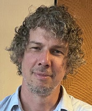 Dr. Daniel Tennant, Rigetting Computing Dr. Daniel Tennant, Rigetting Computing
ABSTRACT: In the last decade, Quantum Information Science has advanced from a mainly academic research topic to a rapidly growing section of the economy. During this time, superconducting qubits have become one of the most promising hardware platforms for near-future quantum computing processors. Devices based on superconducting circuits, cavities, and resonators have leveraged well established fabrication techniques to create a wide variety of structures capable of proof of principle demonstrations of multi-qubit operations, quantum simulations, quantum algorithms, and quantum error correction. In this talk, I will cover some of the fundamentals of superconducting qubit operation and the hardware infrastructure necessary for their operation. Additionally, I will highlight some of the current challenges in the development of this technology as the field progresses towards commercially viable quantum processors.
Dr. Daniel Tennant is a Senior Quantum Engineer at Rigetti Computing, a Full-Stack Quantum Computing company headquartered in the Bay Area. He completed his PhD at the University of Texas in 2017 in the research group of Dr. Raymond Orbach studying magnetic properties of mesoscopic spin glass materials. Afterwards he accepted a joint Postdoctoral Fellow position at the University of Waterloo and MIT Lincoln Laboratories developing technologies for superconducting quantum annealing processors. Following this, he worked at Lawrence Livermore National Laboratory as a Postdoctoral Researcher where his research focused on the detection, identification, and mitigation of noise sources in superconducting quantum devices. He currently utilizes the expertise gained at these research positions to design, test, and produce commercially viable quantum processing units at industry scale.
|
|
Quantum Error Correction in Bosonic Qubits
 Marina Kudra, PhD, Intermodulation Products Marina Kudra, PhD, Intermodulation Products
ABSTRACT: Quantum error correction (QEC) is an essential ingredient of quantum computers. It is an algorithm that lowers the rate of physical qubit errors by redundantly encoding binary quantum information in a multidimensional quantum system. I will explain on a high level what quantum error correction is and give an overview of quantum error correction protocols implemented so far in superconducting circuits. To date, bosonic qubits stand out as the only system that improved qubits’ lifetime by implementing QEC. So we will look into the advantages of bosonic error correction schemes. Finally, I will summarize the challenges we encountered when we implemented parts of the autonomous QEC protocol in a bosonic mode.
Marina Kudra, PhD, works for Intermodulation Products as Quantum Application Specialist helping customers implement their experiments using IMP products. She recently completed her PhD at Chalmers University of Technology in Sweden with the topic Building a Bosonic Microwave Qubit. Her PhD work covered everything from building hardware components of bosonic qubits up to designing a quantum error correction protocol. She did a EMM Nanoscience and Nanotechnology master jointly at KU Leuven in Belgium and Chalmers University of Technology in Sweden. She did a Bachelor program in Electrical Engineering at Belgrade University in Serbia.
|
|
Introduction to Quantum Computing: from Algorithm to Hardware
 Dr. Hiu Yung Wong, San Jose State University Dr. Hiu Yung Wong, San Jose State University
ABSTRACT: Quantum computing is expected to change the world by providing exponential speed-up in solving some very difficult problems. In this tutorial, we will first discuss the fundamental principles of quantum computing algorithms. Error correction, which is essential to realize a fault-tolerant quantum computer, will be briefly covered. Finally, using the superconductor-based quantum computer as an example, we will study how to implement the essential operations in quantum computers, namely, qubit initialization, readout, and manipulations. It will be appreciated that powerful classical computers, which are used to control the qubits, are essential to the successful implementation of quantum computers.
Hiu Yung Wong is an Associate Professor and Silicon Valley AMDT Endowed Chair in Electrical Engineering, at San Jose State University (SJSU). He is the author of the book, “Introduction to Quantum Computing: From a Layperson to a Programmer in 30 Steps”. He is one of the founding faculties of the Master of Science in Quantum Technology at SJSU.
He received his Ph.D. degree in Electrical Engineering and Computer Science from the University of California, Berkeley in 2006. From 2006 to 2009, he worked as a Technology Integration Engineer at Spansion. From 2009 to 2018, he was a TCAD Senior Staff Application Engineer at Synopsys. He received the Curtis W. McGraw Research Award from ASEE Engineering Research Council in 2022, the NSF CAREER award and the Newnan Brothers Award for Faculty Excellence in 2021, and Synopsys Excellence Award in 2010. His works have produced 1 book, 1 book chapter, more than 100 papers, and 10 patents.
|
|
Understanding and Addressing Challenges in Superconducting Qubit Scale
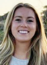 Jennifer Smith, UC-Santa Barbara Jennifer Smith, UC-Santa Barbara
ABSTRACT: Superconducting qubits are a foundational technology for several major industry groups working to build a useful quantum computer including Google Quantum AI, IBM Quantum, and AWS Quantum. These teams have made early advances with superconducting qubits, including the first demonstration of scalable quantum error correction [1] and preliminary evidence for quantum computer utility despite present noise [2]; however, these demo systems must grow 1000x or more to achieve the numbers of logical qubits necessary for meaningful computation. In this talk, I discuss some of the fundamental constraints on system scale arising from the interplay of cryogenics, RF-based control, and superconducting device design and packaging. I will provide a case study on high-density wiring in a cryogenic environment. Lastly, I will discuss advanced multiplexing schemes in control electronics that increase system scale and provide directions for future research.
Jenny Smith has a B.S. in physics from Harvey Mudd College and is currently pursuing a PhD in physics at the University of California, Santa Barbara under Professor Ben Mazin. Her research is focused on improving the system scale and readout signal integrity of thousands of multiplexed superconducting microwave resonators for astronomical imaging. During her PhD, she developed a cryogenic wiring solution that is currently under commercial development by Maybell Quantum Industries. She is also developing a high-throughput control electronics system using the Xilinx RFSoC platform. Outside of academia, she has spent time in industry interning for Xilinx where she worked on open-source high-speed offload designs on the RFSoC platform. She also interned for Google Quantum AI where she worked on superconducting qubit control electronics and wiring. After her PhD, Jenny hopes to pursue a hybrid industry/academic career where she can continue research and development on open-source technologies that enable increasingly performant superconducting array systems.
|
The International Race For A Quantum Computer
 Kristine Boone, PhD, Photonic Inc. Kristine Boone, PhD, Photonic Inc.
ABSTRACT: Silicon transistors, the essential building block of most modern electronic devices, cannot shrink much further without being rendered inoperable by quantum mechanics. This classical-quantum threshold in fact presents a tremendous opportunity: if we harness quantum mechanics, rather than attempt to avoid it, we could build a quantum computer. Quantum computers will open up a new world of opportunities — they could accomplish certain computational tasks exponentially faster which would otherwise be forever impractical. A few recent demonstrations in the US, China and Canada have claimed to have already outperformed the world’s top supercomputers using quantum computers at a few specific computational challenges. During this lecture, Dr. Boone will discuss quantum computing approaches (including Photonic inc’s, based upon CMOS-compatible silicon photonics & spins), how quantum technologies will change our lives in a very fundamental way, and provide a snapshot of the accelerating worldwide race to build a prototype.
Kristine Boone, PhD, works with the outreach and technical teams at Photonic Inc. Prior to the recent move, she was a Business Development Representative for Quantum Engineering Solutions at Keysight Technologies. Dr. Boone started her industry career as a researcher at the quantum computing start-up Quantum Benchmark Inc. (acquired in 2021 by Keysight) and obtained her PhD from the University of Waterloo’s Institute for Quantum Computing (IQC). Her research focused on the characterization of quantum computers, in particular on developing protocols to diagnose error ubiquitously present in quantum computations.
|
|
A 22nm FD-SOI-CMOS Scalable Quantum Processor SoC with Fully Integrated Control Electronics at 3.5K
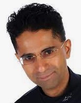 Dr. Imran Bashir, Equal1 Dr. Imran Bashir, Equal1
ABSTRACT: Silicon based Qubits have been proposed as an alternative to Josephson junction structures when it comes to scaling the quantum processor from hundreds to a thousand Qubits. The control electronics in such system needs to generate a unique RF control and DC bias per Qubit without exceeding the thermal budget of the cryocooler. This paper describes a monolithic integration of the semiconductor quantum core and its associated classic control circuitry manufactured in the 22FDX fully depleted silicon-on-insulator (FD-SOI) technology from GlobalFoundries. The quantum control signal is synthesized from a single RF reference clock that drives the pulse generator for timing control and the 8bit capacitive DAC for amplitude control. The on-chip cryogenic memory stores unique patterns to generate various quantum gate behaviors. The readout circuits use a sampled architecture designed to reduce the common-mode and flicker noise in the front-end. In addition, a fully integrated bias generation system using a single input reference is proposed for a moderately complex 2D quantum structure. The combined area of the entire control circuitry is 0.042mm2 while the total power consumption with a reference clock 2.5GHz is 10.7mW at 3.5K.
Imran Bashir received the BSEE degree from the University of Texas at Arlington in 2001 and the MSEE and Ph.D. degrees from the University of Texas at Dallas in 2008 and 2014. He joined Texas Instruments in 2002 and was elected to Group Member of the Technical Staff in 2006. He played a key role in the productization of GSM/EDGE SoCs based on the Digital RF Processor DRPTM technology. In 2009, he joined NVidia Inc. and worked on 2G/3G/4G multi-mode cellular radios. In 2014, he worked as a Mixed-Signal IC Designer with a start-up called Senseeker Engineering Inc. where he designed read-out circuits for IR image sensors. In 2016, he joined Cypress Semiconductor Corp. as an RF/Analog IC design engineer working on connectivity ICs. In August 2019, Imran joined Equal1 Labs Inc. as VP of Analog Engineering and is working on highly integrated and scalable Quantum Processors. Imran has multiple patents and journal papers in the field of Digital Polar Transmitters, Self-Calibration, Interference Mitigation, and Injection Locked Oscillators. In addition to his day-time job, Imran has volunteered as an officer for the IEEE-SSCS, IEEE-CASS, and IEEE-EDS Santa Clara Valley Chapters. He is a member of Tau Beta Pi and Eta Kappa Nu.
|
Network Architecture for a Scalable Spin Qubit Processor
 Prof. Jonathan Baugh, Univ. of Waterloo Prof. Jonathan Baugh, Univ. of Waterloo
ABSTRACT: This talk will focus on electron spin qubits in silicon MOS quantum dots, and the prospects for building a large-scale processor. We propose a node/network architecture for implementing surface code quantum error correction. The scheme splits the scalability problem in two parts: inter-node entanglement distribution and intra-node operations. This approach relaxes constraints on wiring densities and allows the co-integration of cryo-CMOS readout and multiplexing circuits. I will discuss our experimental efforts to simplify the design of Si MOS quantum dots to improve prospects for scalability, as well as the characterization and modelling of cryo-CMOS circuits.
Jonathan Baugh is a Professor of Chemistry at the University of Waterloo, and a faculty member of the Institute for Quantum Computing since 2007. He is an expert in semiconductor nano-electronic devices and quantum information processing, with >74 peer-reviewed publications spanning several areas of quantum nanotechnology research. To date, he has secured over $6.5 million in external research funding and has overseen the mentorship of 36 postdoctoral and graduate researchers. He is a respected member of the quantum community, serving as co-organizer for the Spin Canada workshops in 2017 and 2019. Prior to joining the University of Waterloo, he was a Visiting Researcher at the University of Tokyo and received a PhD in Physics in 2001 from the University of North Carolina at Chapel Hill.
|
|
Quantum Computing with Silicon Spins
 Dr. Dominik Zumbuhl, Univ of Basel Dr. Dominik Zumbuhl, Univ of Basel
ABSTRACT: In this presentation, I will cover recent progress from the NCCR SPIN, the Swiss National Program on Quantum Computation with silicon and germanium spin qubits. Some of the highlights include ultrafast qubit operation, taking only 1 ns to coherently rotate a spin from pointing up to down; operation of spin qubits at temperatures up to 5 K, where vast cooling power becomes available, making possible future on-chip integration of the classical control electronics; and finally demonstration of sweet spots with strongly enhanced coherence and operation of a 2-qubit gate with highly anisotropic exchange, allowing for high fidelity gate operation while operating at high speeds.
Dr. Dominik Zumbuhl, Univ of Basel: After a Physics Diploma from ETH Zürich and MSc from Stanford University, Dominik received his PhD at Harvard University in 2004 on quantum coherence and spin in semiconductor quantum dots. After a brief postdoc at MIT, Dominik started his own group in 2006 at the University of Basel where he has been working since. In 2008, he received a starting grant in the first ERC call. He was promoted to associate professor in 2012 and to full professor in 2023. He served as Department Chair from 2015-2019 and since 2021, he is the director of the NCCR SPIN, the Swiss National Program on Quantum Computing with Si and Ge spins. Dominik’s research interests are in quantum transport experiments in semiconductor nanostructures, focusing on quantum computation with spins, coherence, interactions, quantum condensed matter at ultralow temperatures and machine learning for quantum devices.
|
Superconducting Multi-Chip Module (SMCM)
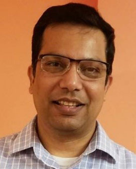 Dr. Rabindra N. Das, MIT Lincoln Laboratory Dr. Rabindra N. Das, MIT Lincoln Laboratory
ABSTRACT: Superconducting single-flux-quantum-based (SFQ) digital integrated circuits (ICs) are a promising candidate for a high speed and ultra-low energy dissipation computing system. Circuits based on several versions of SFQ-type logic, RQL (Reciprocal Quantum Logic), and AQFP( Adiabatic Quantum-Flux-Parametron) logic have been demonstrated with complexities reaching up to a few hundreds of thousands of gates. Packaging many superconducting ICs — and performing fast and nearly lossless operations between SFQ, RQL, AQFP, and CMOS -– is critical for a scalable computing architecture. In this talk, I will present a micro-bump based passive superconductive multi-chip module (SMCM) which distributes information between integrated circuits utilizing impedance controlled, lossless superconducting transmission lines.
This research was funded by the Intelligence Advanced Research Projects Activity (IARPA), and by the Assistant Secretary of Defense for Research & Engineering under Air Force Contract No. FA8702-15-D-0001. (The views and conclusions contained herein are those of the authors and should not be interpreted as necessarily representing the official policies or endorsements, either expressed or implied, of the IARPA, or the U.S. Government.)
Dr. Rabindra Das is a Member of the Technical Staff in the Quantum Information and Integrated Nanosystems Group, MIT Lincoln Laboratory, Lexington, MA. Prior to MIT, he was a Principal Engineer at Endicott Interconnect Technologies (formerly IBM Endicott). Dr. Das has 20 years of experience in microelectronics packaging development for applications ranging from HPC to medical to quantum electronics. He holds 48 patents and more than 100 publications.
|
|
NVIDIA cuQuantum SDK: Accelerating Quantum Circuit simulation II – cuStateVec
 Dr. Shinya Morino, Nvidia Tokyo Dr. Shinya Morino, Nvidia Tokyo
ABSTRACT: The cuStateVec library is a part of NVIDIA’s cuQuantum SDK and accelerates state vector simulations on NVIDIA GPUs. It provides APIs to accelerate gate applications, sampling, and other common operations in state vector simulations on single GPUs. The library also provides APIs to scale out state vector simulations on multiple GPUs and multiple nodes. Two cuStateVec-based simulators are released in the NVIDIA cuQuantum Appliance for IBM’s Qiskit/Qiskit-Aer with multi-node support and Google’s Cirq/qsim with multi-GPU support. This presentation will describe the use cases of the cuStateVec API in these simulators and the optimizations to realize large-scale high-performance state vector simulations.
Shinya Morino is a principal software engineer in the CUDA Math Libraries group at NVIDIA. He joined NVIDIA in 2013 and engaged CUDA trainings and developer support in various industrial fields as a solution architect. As a developer of a quantum computing simulator, he has prototyped a GPU-accelerated state vector simulator in the NVIDIA AI Technology center. With the launch of cuQuantum, he joined cuQuantum development and moved to the CUDA Math Libraries group to drive cuStateVec development. Shinya holds a Ph.D in engineering from the University of Tokyo, Japan.
|
Cryo-CMOS Transceivers for Control and Readout of Semiconductor Spin Qubits
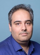 Masoud Babaie, Associate Professor, Delft University of Technology Masoud Babaie, Associate Professor, Delft University of Technology
ABSTRACT: A fault-tolerant quantum computer operates at deep cryogenic temperatures (typically 20-100mK) and requires massive yet very precise control electronics for the manipulation and read-out of individual quantum bits (qubits). The most complex state-of-the-art quantum computer (with 53 qubits) requires tens of bulky custom-made electronic modules operating at room temperature and connected to cryogenic qubits via hundreds of coaxial cables. However, this approach is not practical for implementing fault-tolerant quantum computers with millions of qubits due to the utter interconnect complexity, poor system scalability, and reliability. A better alternative would be to integrate the qubits and the control electronics on the same die or package and operate them at the same temperature. Toward this goal, electronics able to operate at cryogenic temperatures in close proximity to the qubits must be developed.
In this presentation, the system-level specifications for control and readout electronics are first discussed. Then, we review the characteristics and behavior of CMOS active and passive components at cryogenic temperatures. By exploiting the developed CMOS and qubit models, we develop the block diagram and circuit schematic of a digitally intensive wideband transmitter capable of operating at 3K and controlling 32 frequency-multiplexed qubits. It also offers waveform shaping flexibility, minimum execution latency, and straightforward integration in the existing quantum computing stack. The cryogenic controller is used to coherently control actual qubits encoded in the spin of single electrons confined in silicon quantum dots. Then, we shift the gear towards the challenges in the design of a cryogenic-CMOS (Cryo-CMOS) receiver for the gate-based readout of spin qubits. Finally, after showing the electrical performance, the cryo-CMOS receiver is used to measure the DQD charge stability diagrams and quantify the maximum achievable SNR of the gate-based readout architecture. These results open up the way towards a fully integrated, scalable silicon-based quantum computer.
Masoud Babaie is currently an Associate Professor at the Delft University of Technology, Delft, The Netherlands. His research interests include RF/millimeter-wave integrated circuits for wireless communications and cryogenic electronics for quantum computation. Dr. Babaie currently serves as a technical program committee (TPC) member of the ISSCC and ESSCIRC conferences. He was a co-recipient of the 2019 IEEE ISSCC Demonstration Session Certificate of Recognition, the 2020 IEEE ISSCC Jan Van Vessem Award for Outstanding European Paper, the 2022 IEEE CICC Best Paper Award, the 2023 IEEE IMS Best student paper award. In 2019, he received the Veni Award from the Netherlands Organization for scientific research.
|
|
Thermal Management Challenges in Cryogenic System Integration: Spin Qubit Biasing with a CMOS DAC at mK Temperature
 Lea Schreckenberg, Forschungszentrum Jülich GmbH Lea Schreckenberg, Forschungszentrum Jülich GmbH
ABSTRACT: To pave the way of integrating millions of qubits to run advanced algorithms on a universal quantum computer, a scalable control and read out of these qubits is crucial for the overall system. Due to the wiring in state-of-the-art dilution refrigerators (DR), the systems’ scalability with room temperature electronics is strictly limited. From our perspective, the approach of placing cryogenic electronics on the intermediate 4K stage of a DR is shifting the wiring bottleneck from room temperature to 4K without tackling the challenge at hand of wiring towards the mixing chamber (MC). Having integrated circuits (ICs) operating next to the qubits at mK temperatures could represent a solution to solve the scalability challenge. However, the development of innovative strategies for cryogenic circuits becomes essential.
Based on this, the talk will give an overview about the recent activities of our custom designed CMOS demonstrator in form of a scalable, fully integrated, eight channel Bias-DAC designed in a 65-nm bulk CMOS technology co-integrated at the MC plate with different gate defined spin qubit devices. We present the DC bias of a single electron transistor as well as a single and double quantum dot bias of one of the qubit devices with the DACs power consumption of about 20 uW. This is framed by a detailed review of different setup iterations with respect to power dissipation and the resulting temperature dependencies. The usage of an interposer as a future System in Package (SiP) chip carrier shows new challenges for a quantum processor unit (QPU) underlined by measurement results with different materials and assemblies. Thus, we emphasize the systems requirement to connect the IC and the qubit device electrically while thermally isolating them from
the carrier.
Lea Schreckenberg is a postgraduate researcher working at the Central Institute of Engineering, Electronics and Analytics – Electronic Systems (ZEA-2) at the research center Jülich. She received her masters degree in electrical engineering at the University of Applied Sciences Aachen in 2020. She is focusing on the integration of scalable control electronics with spin qubit devices for quantum computing for her doctoral research, with interests in cryogenic characterization and thermal management.
|
Photonics Integrated Circuits for Quantum and Beyond
 Dr. Minh Tran, Director or Research, Nexus Photonics Dr. Minh Tran, Director or Research, Nexus Photonics
ABSTRACT: In the fast-paced world of quantum computing, the demand for scalable and adaptable technology platforms continues to grow. Nexus Photonics is at the forefront of this change, offering a photonics platform that not only holds promise for quantum applications but also advocates for a significant reduction in size, weight, and power (SWAP), promoting cost-efficiency and scalability in mass production using the CMOS process. In this presentation, I will outline the developments in our Photonics Integrated Circuits (PICs), highlighting their potential in paving the way for innovations in the quantum computing sector and beyond.
Dr. Minh Tran earned his B.S. degree in Electrical Engineering from the University of Tokyo in 2013. Following the completion of his Ph.D. at the University of California at Santa Barbara in 2018, he joined Nexus Photonics as a founding employee and has since ascended to the role of Director of Research. Over the years, he has been instrumental in the development of numerous record-setting devices in the field of integrated photonics, including an integrated semiconductor laser characterized by a record-breaking ultra-wide wavelength tuning range and ultra-narrow intrinsic linewidth. Furthermore, he has contributed as an author or co-author to a series of patents in the fields of heterogeneous photonics, narrow-linewidth lasers, and high-Q resonators.
|
|
Fully-integrated Cryo-CMOS Spin-to-digital Readout for Spin Qubits
 Michele Castriotta, Politecnico di Milano Michele Castriotta, Politecnico di Milano
ABSTRACT: We have successfully fabricated and characterized a fully-integrated CMOS readout that operates at cryogenic temperatures for semiconductor spin qubits. Our readout achieves a comparable or even smaller single-shot readout time compared to RF-reflectometry. It is based on a direct spin-to-digital conversion, which includes a gated integrator for sensing the spin dependent current from a single-electron transistor and a programmable self-calibrated comparator to provide a digital output of the spin measurement. Our cryogenic comparator integrates CMOS-compatible floating-gate transistors as memory element to obtain a low-power and compact threshold, which is self-calibrated during an initialization phase to improve the detection accuracy. With our readout, we can resolve a variation of the sensing current of 250 pA with a sub-microsecond time resolution and a fidelity of 99.86%. What’s more, our readout consumes only 1.2 mW of power and occupies an area of less than 0.04 mm2.
Our solution doesn’t require off-chip components and the handling of microwave signals, which makes it more compact and reliable compared to the most common RF-reflectometry readout techniques. As a result, our approach exhibits promising scalability, particularly in scenarios where the co-integration of quantum processing units and readout electronics is feasible on a shared cryogenic board.
Michele Castriotta is a Ph.D student in Information Technology at the Department of Electronics, Information and Bioengineering (DEIB) of Politecnico di Milano, Italy. He received the M.Sc. (2020) Degrees in Electronics Engineering from Politecnico di Milano. His current research field is related to the development of very low noise instrumentation for high sensitivity electrical measurements at cryogenic temperature. He also investigates the aspects of the quantum transport in nano-scale devices.
|
Readout of Spins in Silicon
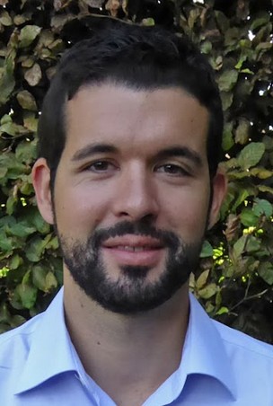 Dr. M. Fernando Gonzalez-Zalba, Quantum Motion Technologies Dr. M. Fernando Gonzalez-Zalba, Quantum Motion Technologies
ABSTRACT:Spin qubits in silicon are a promising platform for scalable quantum computing due to their small footprint, VLSI compatibility and demonstrated operation fidelities above fault-tolerant thresholds. In the path to scaling, a key aspect is developing compact and fast high-fidelity readout techniques to enable highly connected qubit architectures as well as mid-circuit measurements, a necessary feature for many dynamic algorithms and quantum error correction. In this talk, I will introduce the concept of radio-frequency reflectometry for fast readout of spin qubits as a method to achieve the goal. By embedding the devices in radio- or microwave-resonant circuits, high-bandwidth and novel compact methods for readout can be implemented. I will review the state-of-the-art of the field and present a series of results that highlight improvements at all stages of the readout chain that enable achieving readout fidelities above fault-tolerant thresholds in timescales comparable to the gate operation times. First, at the device level, I will describe optimal device fabrication recipes and introduce methods to abstract spin qubit devices into classical circuit elements for efficient simulation. Then, at the resonator level, I will present optimized designs tailored to the specific measurement method. At the amplifier level, I will discuss quantum-limited techniques specific for spin qubit devices. Finally, I will show spin relaxation measurements as well as two-qubit coherent control using dispersive readout methods.
Dr. Fernando Gonzalez-Zalba is a Principal Quantum Engineer and heads the Quantum Hardware team at Quantum Motion Technologies, a UK-based start-up dedicated to the development of quantum computing hardware based on silicon technology. Fernando is also an UKRI Future Leader Fellow, Associated Lecturer at the University of Cambridge, Research Associate at University College London, and Quondam Fellow at Hughes Hall, a Cambridge College. Fernando’s research focuses on a variety of topics such as single-atom electronics, quantum sensing, quantum-limited amplification, cryogenic classical electronics, and new computing paradigms such as quantum computing. Prior to that Fernando obtained a PhD from the University of Cambridge with a thesis on Single-atom Electronics in 2013 and was Head of Quantum Computing at the Hitachi Cambridge Laboratory, a R&D centre of Hitachi Europe. His research has been funded by the European Commission’s FP7 and H2020 programmes, Innovate UK, EPSRC, the Winton Programme for the Physics of Sustainability and the Royal Society totalling more than £5.0M.
|
|
A Scalable Architecture for Integrating Spin Qubits with Cryogenic Electronics
 René Otten, Forschungszentrum Jülich GmbH René Otten, Forschungszentrum Jülich GmbH
ABSTRACT: Spin Qubits are quickly emerging as one of the most promising platforms for a scalable quantum computing system, mainly due to increasing qubit numbers and fidelities compatible with quantum error correction. However, scaling beyond lab-scale systems to millions of qubits remains an open challenge. In this talk, I will elaborate on our plan to tackle this problem using a highly scalable architecture and cryogenic electronics. Our approach increases the native pitch of spin qubits from the nm regime to tens of um with minimal wiring overhead, matching the qubit pitch with the space requirements of cryogenic control electronics. I present details on our architecture, which is based coherent shuttling of electrons and how it can reduce the number of necessary control signals per area. To emphasize the validity of our approach, I will present the results of EPR-pair separation in a shuttling device recently measured in our lab.
Subsequently, I will briefly review recent results using a cryogenic CMOS-DAC to generate bias voltages for spin qubits, and the use of discrete heterojunction bipolar transistors (HBTs) for readout. For the first, we successfully operated a custom-designed DAC on the mixing chamber of our cryostat next to the qubit device. Extrapolating the DAC’s performance, we find that we should be able to push the power consumption for DC voltage generation to less than 100 pW/ch. For the HBTs, I will discuss our efforts to minimize the power consumption of these discrete transistors used for spin qubit readout, building on work previously developed by other research groups. I will conclude the talk with our plan on how to integrate spin-qubits with cryogenic electronics in a single QPU, touching on issues such as wiring concepts, thermal design, and packaging.
René Otten is at the JARA Institute for Quantum Information, Forschungszentrum Jülich GmbH and RWTH Aachen University, Aachen, Germany. He received his doctoral, M.Sc., and B.Sc degrees in physics from RWTH Aachen University, Germany, in 2023, 2017, and 2015 respectively. His dissertation at a joint institute with the Forschungszentrum Jülich GmbH focused on integrating semiconductor spin qubits with electronics at cryogenic temperatures. He is currently building up a group on cryogenic electronics for quantum computation as part of the JARA Institute for Quantum Information and RWTH Aachen University. In 2022, he also joined the local start-up ARQUE Systems building scalable quantum computers based on spins in semiconductors. His research focuses on scalable quantum computing systems based on semiconductors. This includes CMOS electronics in cryogenic environments and the integration of spin qubits in semiconductor quantum dots with cryogenic electronics.
|
Power Integrity Challenges in Large Scale Quantum Computers and Solutions
 Alfonso R. Cabrera-Galicia, Forschungszentrum Jülich GmbH Alfonso R. Cabrera-Galicia, Forschungszentrum Jülich GmbH
ABSTRACT: The ICs belonging to a quantum computer need stable and regulated supply voltages for proper operation, e.g. the phase noise of RF oscillators is dependent on their power supply quality. Moreover, the power supply needs of a large scale QC will be challenging to satisfy by simply using supply lines connecting the ICs inside the cryostat with the power sources at room temperature. This is because voltage ripples (e.g. pulse tube vibration induced noise), ground loops induced noise and dynamic load currents may affect the ICs supply lines and compromise the QC power integrity. Furthermore, it is expected that the connection lines available in large scale QCs be scarce due to the limited cryostat space. Therefore, the usage of several lines to set different supply domains may not be possible and be a restricting factor for the QCs scalability.
This presentation will address the cryogenic power integrity topic by providing: — A review of the power integrity challenges faced by cryogenic ICs. — Solution approaches focused on the cryogenic setup and the use of cryogenic voltage regulators. — Cryogenic characterization and modelling of FDSOI technology (22 nm) for ICs design. — Design and test of cryogenic voltage references, based on cryogenic Vth saturation and Vth difference. — Design and test of a cryogenic voltage regulator. — Design of Digital LDOs for cryogenic applications. — An application case: cryogenic voltage regulator applied to power the reference circuit of a cryogenic DAC used for the DC voltage setting of a Single Electron Transistor Quantum Dot
Alfonso Rafael Cabrera-Galicia develops research activities on the design and test of cryogenic electronic systems for quantum computing as PhD researcher of the Central Institute of Engineering, Electronics and Analytics, Electronic Systems – ZEA-2, Forschungszentrum Jülich GmbH, Germany.
He holds the M.Sc. degree in electronics from the Instituto Nacional de Astrofísica, Óptica y Electrónica (INAOE), México, and currently he is pursuing his Ph.D. degree at the University of Duisburg-Essen, Germany. His current research interest includes the design and test of analog integrated circuits, analog/mixed-signal processing and cryogenics.
|
|
Challenges of Cryogenic CMOS Controller for Qubits
 Chia-Hsin Lee, Taiwan Semiconductor Research Institute (TSRI) Chia-Hsin Lee, Taiwan Semiconductor Research Institute (TSRI)
ABSTRACT: The cryo-CMOS control interface circuits are a key enabling technology for the scale-up of quantum computers. To achieve a fidelity of Qubit operation greater than 99.99%, this controller chip needs to perform well with low noise and a Spur-Free Dynamic Range (SFDR) that is larger than 45 dB. Also, the power consumption per channel should be within a few milliwatts to support more Qubits at the 4 K stage. In this talk, the design and measurement challenges of analog, digital, and RF circuits, which are used in the Qubit controller design, are discussed and presented.
At 4 K temperature, the higher MOS threshold voltage (Vth) adds difficulties to analog circuit bias, especially for modern advanced technology nodes. Also, high Vth combined with reduced routing resistance makes the transient time and propagation delay values in the digital synthesis library unreliable and leads to malfunctions in the digital test chip at 4 K temperature. To mitigate the challenges of cryogenic circuit design, putting efforts into 4 K SPICE modeling is essential for a successful implementation of analog and digital circuits. Therefore, the importance of device modeling at 4 K temperature will be presented. In addition, the design experiences of certain controller circuit blocks are provided to explain the significance of bias and power management. Finally, the setups and peripherals to support reliable 4 K circuit measurements are also shown for completeness.
Chia-Hsin Lee Chia-Hsin Lee received the B.S. and M.S. degrees in electrical engineering from the National Cheng Kung University (NCKU), Tainan, Taiwan, in 2014 and 2016, respectively. She is currently an electronics engineer with the Taiwan Semiconductor Research Institute (TSRI), National Applied Research Laboratories (NARL), Tainan, Taiwan. Her research interests include cryogenic analog circuits, read-out circuits for optical sensors, and high-speed SAR ADCs.
|
Integrated Quantum: Classical Applications with CUDA Quantum
 Dr. Jin-Sung Kim, NVIDIA Dr. Jin-Sung Kim, NVIDIA
ABSTRACT: A critical challenge to leveraging the computational advantages of a future quantum processor is to effectively combine it with the best existing classical computing infrastructure. A key tool for enabling hybrid quantum-classical research and application development is a programming model and software toolchain which allow researchers to straightforwardly co-program classical and quantum computers and leverage the best tools available for each. CUDA Quantum is a single-source programming model in C++ and Python for heterogeneous quantum-classical computing. The CUDA Quantum platform provides several advantages and new capabilities that enable users to get more out of quantum processors.??Here, CUDA Quantum is discussed in the context of a quantum chemistry application, the Variational Quantum Eigensolver (VQE) where it provides a significant (~287x) performance and capability benefit over existing quantum programming paradigms.
Jin-Sung Kim is the Developer Relations Manager for Quantum Computing at NVIDIA and is based out of San Francisco. In his current role, he manages partnerships, technical collaborations and the rapidly growing NVIDIA Quantum ecosystem. Prior to NVIDIA, he was a Research Staff Member at IBM Quantum. Jin-Sung holds a PhD from Princeton University.
|
|
NVIDIA cuQuantum SDK: Accelerating Quantum Circuit Simulation I – cuTensorNet
 Dr. Azzam Haidar, Nvidia Tennessee Dr. Azzam Haidar, Nvidia Tennessee
ABSTRACT: We present the NVIDIA cuQuantum SDK, a state-of-the-art library of composable primitives for GPU-accelerated quantum circuit simulations. The cuQuantum SDK was created to accelerate and scale-up quantum circuit simulators developed by the quantum information science community by enabling them to utilize efficient scalable software building blocks optimized for NVIDIA GPU-based platforms. The functional building blocks provided cover the needs of both state vector- and tensor network-based simulators, including approximate tensor network simulation methods based on matrix product state, projected entangled pair state, and other factorized tensor representations. By leveraging the enormous computing power of the latest NVIDIA GPU architectures, quantum circuit simulators that have adopted the cuQuantum SDK demonstrate significant acceleration, compared to CPU-only execution, for both the state vector and tensor network simulation methods.
Bio: Azzam Haidar is a principal engineer at NVIDIA developing HPC and Quantum Computing software. He received a Ph.D. in 2008 major Computer Science and Applied Mathematics from the National Polytechnic Institute of Toulouse and from the CERFACS Lab, France. Before joining NVIDIA, he was a Research Director at the Innovative Computing Laboratory at the University of Tennessee, Knoxville. Azzam has a strong background in numerical mathematics, with interests focusing on the development, optimization and implementation of parallel scalable HPC libraries for distributed multicore/GPU-based architectures, for extreme-scale scientific applications. He is also working on developing algorithms and techniques to help making quantum simulation and synthesis feasible on current computer hardware.
He has an interest in developing optimized kernels for Deep Learning algorithm and studying techniques to speedup the learning process. He also developed novel algorithms for singular value (SVD) and eigenvalue problems as well as approaches that uses data flow representations to express parallelism in scientific applications.
|
Introduction to Quantinuum and TKET
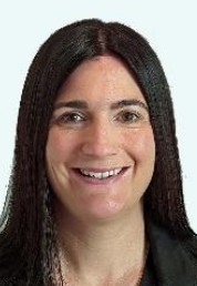 Dr. Kathrin Spendier, Quantinuum Dr. Kathrin Spendier, Quantinuum
ABSTRACT: Quantinuum, a full-stack quantum computing company, integrates state-of-the-art trapped-ion quantum computing hardware and software to deliver solutions across various applications, including drug discovery, materials science, and finance. The company serves as a center of gravity in the quantum computing world, fostering widespread collaboration. This is facilitated by the development of “TKET”, an open-source, architecture-agnostic quantum software development kit, including a state-of-the-art compiler. This technology enables partners, collaborators, and clients to operate seamlessly across multiple platforms, tackling some of the most complex and intriguing challenges in quantum computing.
Dr. Kathrin Spendier is a Quantum Evangelist at Quantinuum, where she promotes the company’s advanced open-source quantum software development kit, TKET. Her role involves active engagement with the quantum computing community, providing resources and support for users, and driving TKET’s adoption through educational outreach and community engagement. Prior to her role at Quantinuum, Dr. Spendier was an Associate Professor in the Physics Department at the University of Colorado Colorado Springs. During this time, she conducted extensive research in biophysical phenomena and condensed matter physics and developed and taught various undergraduate and graduate physics courses. Dr. Spendier holds a Ph.D. in Physics from the University of New Mexico.
|
|
NVIDIA cuQuantum SDK: Accelerating Quantum Circuit Simulation II – cuStateVec
 Dr. Shinya Morino, Nvidia Tokyo Dr. Shinya Morino, Nvidia Tokyo
ABSTRACT: The cuStateVec library is a part of NVIDIA cuQuantum SDK and accelerates state vector simulations on NVIDIA GPU. It provides APIs to accelerate gate applications, sampling, and other common operations in state vector simulations on single GPU. The library also provides APIs to scale out state vector simulations on multiple GPUs and multiple nodes. Two cuStateVec-based simulators are released in NVIDIA cuQuantum Appliance for IBM’s Qiskit/Qiskit-Aer with multi-node support and Google’s Cirq/qsim with multi-GPU support. This presentation will describe the use cases of the cuStateVec API in these simulators and the optimizations to realize large-scale high-performance state vector simulations.
Bio: Shinya Morino is a principal software engineer in CUDA Math Libraries group at NVIDIA. He joined NVIDIA in 2013 and engaged CUDA trainings and developer support in various industrial fields as a solution architect. As a developer of a quantum computing simulator, he has prototyped a GPU-accelerated state vector simulator in NVIDIA AI Technology center. With the launch of cuQuantum, he joined cuQuantum development and moved to the CUDA Math Libraries group to drive cuStateVec development. Shinya holds a Ph.D in engineering from the University of Tokyo, Japan.
|
Nonlinear Integrated Photonics for Quantum Communications and Computing
 Trevor Steiner, UC-Santa Barbara Trevor Steiner, UC-Santa Barbara
ABSTRACT: The development of scalable optical technologies for quantum communications, computing, and precision measurements requires reducing existing table-top experiments to fully integrated chip-scale photonic circuits. We utilize several approaches, including AlGaAs-on-insulator, silicon nitride, and III-Vs on silicon, that combine ultra-bright deterministic and probabilistic quantum light sources with ultra-low-loss photonic circuits, passive and active components, and superconducting nanowire single-photon detectors. In this talk, I will highlight our record-high entangled photon pair brightness using AlGaAsOI microring resonators as well as show some of our application-focused works that are currently ongoing.
Trevor Steiner is a fifth year Materials PhD student at the University of California Santa Barbara advised by Professor John Bowers and Professor Galan Moody. His work focuses on nonlinear integrated quantum photonics using III-V semiconductor materials. In 2021, he demonstrated an ultrabright entangled photon pair source from AlGaAsOI microring resonators that is over 1000 times more efficient than state-of-the-art SOI quantum light sources. Since this work, he has been focusing on developing integrated circuits using these efficient sources as well as using these sources for applications like quantum key distribution and quantum frequency information processing. Trevor is an NSF Quantum Foundry Fellow and a recipient of the Institute for Energy Efficiency Excellence in Research Fellowship.
|
|
Register today!

|

 Dr. Daniel Tennant, Rigetting Computing
 Marina Kudra, PhD, Intermodulation Products
 Dr. Hiu Yung Wong, San Jose State University
 Jennifer Smith, UC-Santa Barbara
 Kristine Boone, PhD, Photonic Inc.
 Dr. Imran Bashir, Equal1
 Prof. Jonathan Baugh, Univ. of Waterloo
 Dr. Dominik Zumbuhl, Univ of Basel
 Dr. Rabindra N. Das, MIT Lincoln Laboratory
 Dr. Shinya Morino, Nvidia Tokyo
 Masoud Babaie, Associate Professor, Delft University of Technology
 Lea Schreckenberg, Forschungszentrum Jülich GmbH
 Dr. Minh Tran, Director or Research, Nexus Photonics
 Michele Castriotta, Politecnico di Milano
 Dr. M. Fernando Gonzalez-Zalba, Quantum Motion Technologies
 René Otten, Forschungszentrum Jülich GmbH
 Alfonso R. Cabrera-Galicia, Forschungszentrum Jülich GmbH
 Chia-Hsin Lee, Taiwan Semiconductor Research Institute (TSRI)
 Dr. Jin-Sung Kim, NVIDIA
 Dr. Azzam Haidar, Nvidia Tennessee
 Dr. Kathrin Spendier, Quantinuum
 Trevor Steiner, UC-Santa Barbara