2025 Build-Up Substrate Symposium
| ADVANCE PROGRAM | ||
| Thursday, May 8, 2025 | ||
| Time | Speaker | Title/Abstract |
| 7:45 | Registration and coffee/pastries | |
| 8:45 | Welcome and Introduction | |
| Keynote Addresses | ||
| 9:00 |  Sai Boyapati, Director of Technology Development, AMD Advanced Packaging Sai Boyapati, Director of Technology Development, AMD Advanced Packaging
|
Advanced Packaging Substrate Technologies for Power Efficient AI Products — This talk outlines the AMD advancements in power-efficient AI through advanced packaging technologies. It highlights AMD’s end-to-end portfolio, including processors, GPUs, and accelerators designed for various applications from endpoints to cloud computing. Then it discusses the challenges of traditional Moore’s Law scaling, increasing costs, and thermal impacts … (more) |
| 9:40 |  E. Jan Vardaman, President and Founder, TechSearch International, Inc. E. Jan Vardaman, President and Founder, TechSearch International, Inc.
|
Substrate Market Outlook — Substrates are essential for IC packagers. For high performance applications such as AI, server CPU, and network switches build-up substrates with multiple layers are required. Automotive requires substrates that meet special reliability requirements. Many of high-performance packages use a silicon or redistribution layer (RDL) … (more) |
| 10:00 | Coffee/Tea and Networking | |
| Session 1: Substrate Challenges for Chiplet Integration Chair: Rozalia Beica, Rapidus |
||
| 10:40 |  Venkata Mokkapati, Director, Business Development & Application Engineering, AT&S AG Venkata Mokkapati, Director, Business Development & Application Engineering, AT&S AG
|
Addressing New Challenges with Conventional Organic Substrates — The industry has been looking for alternative solutions to address substrate challenges, especially integration on larger packages which are even beyond current Jedec standards. There are several technologies that have been proposed which could solve these problems, organic solutions for example … (more) |
| 11:00 | 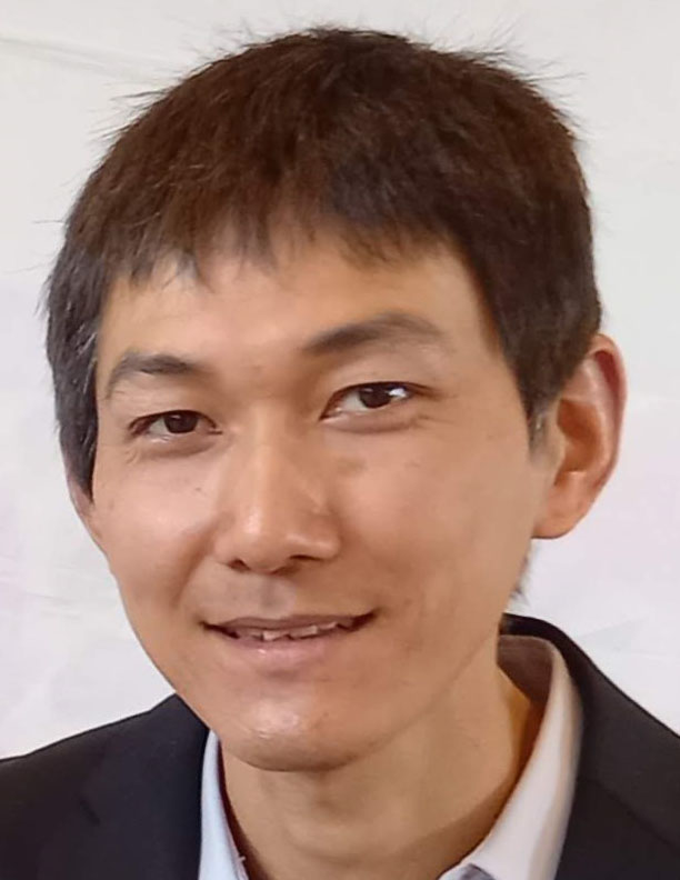 Shingo Hayashibe, Shinko Electric America, Inc. Shingo Hayashibe, Shinko Electric America, Inc.
|
Large Form Factor Chiplet Package using an Organic Interposer for Chip-last Assembly — Interposers that integrate multiple semiconductor chips are rapidly becoming larger. SHINKO’s i-THOP, an organic interposer with 2.3D structure, using semiconductor thin-film technology and Shinko’s assembly processes is one solution for these large size interposers … (more) |
| 11:20 | 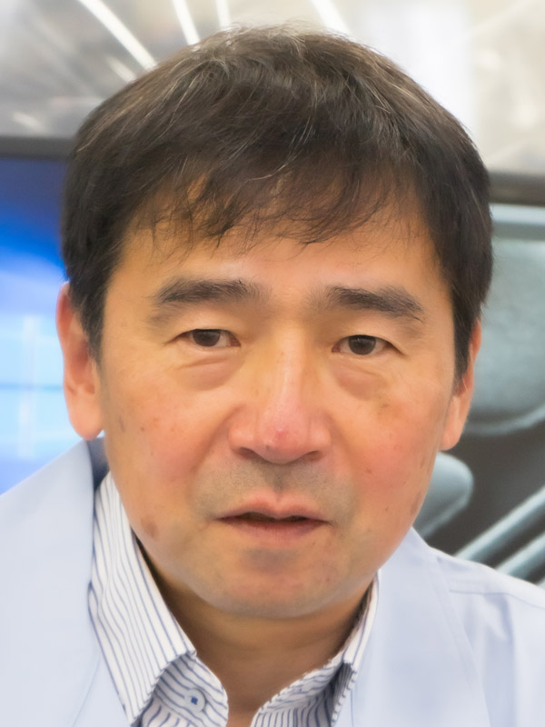 Satoru Kuramochi, Research Fellow, Fine Packaging Division, Dai Nippon Printing Co. (DNP) Satoru Kuramochi, Research Fellow, Fine Packaging Division, Dai Nippon Printing Co. (DNP)
|
Large Scale Glass Substrate for High Performance Computing Application — As the industry moves toward High Performance Computing (HPC) for huge data transmission with low power consumption. The requirements for PKG structure have become more challenging. The major engineering requirements for HPC application are high-density, high-speed data transmission … (more) |
| 11:40 |  Vern Stygar, AGC Vern Stygar, AGC
|
Glass Compositions for Data Centers, AI, and Quantum Computing — The use of glass as a core material for electronic and photonic packaging substrates is being considered due to its rigidity, flatness, and dimensional stability for advanced packaging such as chiplet packaging requiring large format and high-density interconnection. This presentation will provide an overview of glass material technology, processing technology and the need for reliability testing for glass core substrates … (more) |
| 12:00 | Lunch (from DishDash) | |
| Session 2: Materials for Substrates Chair: Annette Teng, NY Creates |
||
| 13:00 |  Shiro Tatsumi, Ajinomoto Shiro Tatsumi, Ajinomoto
|
Advanced Insulation Material for High Performance Semiconductor Packages — Printed circuit boards such as multi-layer printed wiring boards and flexible printed wiring boards are used for a wide variety of electronic devices. Ajinomoto Build-up Film®(ABF) has been widely utilized for a variety of package structures due to its outstanding insulation reliability, good resin flow, thickness uniformity and Semi-Additive Process (SAP) compatibility for fine line and space formation. Low coefficient of thermal expansion (CTE) … (more) |
| 13:20 |  Yuya Suzuki, Taiyo America Yuya Suzuki, Taiyo America
|
Dry-film Solder Resist Materials for High Density IC Substrates — The demand for high-density integrated circuit (IC) substrates is driving advancements in material technologies to meet the increasing complexity and performance requirements of high-performance electronics. Solder resist (SR) materials play a critical role in IC substrate applications by providing insulation and protecting circuit patterns… (more) |
| 13:40 |  Hikaru Mizuno, JSR Micro Hikaru Mizuno, JSR Micro
|
Advanced Photo-imageable Dielectric Film Enabling Sub-5-micron Patterning for Next Generation Build-up Layer — As novel electronic products become dramatically smaller and more highly functionalized, semiconductor packaging structures are also required to become smaller, thinner and more complicated. Based on these market trends, the IC substrate has become one of the most important components in packaging. Next-generation build-up layer patterning materials for IC substrates are required to meet the demands of ultra-fine via patterning… (more) |
| 14:00 | 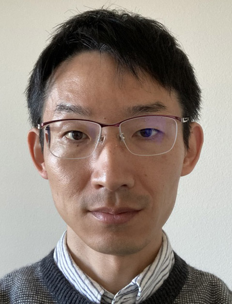 Masa Fukui, Resonac America, Inc. Masa Fukui, Resonac America, Inc.
|
The Development of Organic Substrate Materials for Advanced Packaging — The development of advanced packaging technology has been accelerated, such as for 2.5D packaging and chiplet design. Advanced packaging requires HSIO, high density interconnection and large form factor. This motivation for future packaging is the driving force behind the development of substrate materials to meet the challenges. In this perspective, glass substrates are considered as the future generation substrate … (more) |
| Session 3: Emerging Substrate Technologies Chair: Steven Verhaverbeke, Applied Materials |
||
| 14:20 |   Jason Conrad, Arizona State University, and Craig Bishop, Chief Technology Officer, Deca Technologies Jason Conrad, Arizona State University, and Craig Bishop, Chief Technology Officer, Deca Technologies
|
SHIELD USA: Leap-ahead Organic Substrate Technology — The CHIPS Act renewed a domestic focus on semiconductor technology, including advanced packaging that is critical for chiplets and future scaling. Under the National Advanced Packaging Manufacturing Program (NAPMP), ASU is leading the Substrate-based Heterogeneous Integration Enabling Leadership Demonstration for the USA (SHIELD USA) program … (more) |
| 14:40 |  Sung Jin Kim, Ph.D., CTO, Absolics Sung Jin Kim, Ph.D., CTO, Absolics
|
Transforming Semiconductor Packaging with Glass-Based Substrates — The packaging substrate industry is encountering unprecedented challenges driven by the rapid evolution of semiconductor applications, particularly in artificial intelligence (AI), high-performance computing (HPC), and high-frequency radio frequency (RF) systems. As device complexity and performance requirements escalate, addressing critical build-up package substrate challenges … (more) |
| 15:00 |  Steven Verhaverbeke, Applied Materials Steven Verhaverbeke, Applied Materials
|
Wafer-Level Si Core Substrates – Third Leg of the NAPMP Substrates Program — The rise of chiplet and 2.5D packaging has been driven by the increasing demands for higher performance, scalability, and power efficiency in modern semiconductor design. As Moore’s Law slows, traditional monolithic scaling becomes less viable due to cost and yield challenges. 2.5D packaging, which utilizes an interposer to connect multiple chiplets… (more) |
| 15:20 | Coffee/Tea and Networking | |
| 16:00 | Panel: Technology Development R&D Centers of Excellence | Moderators: Jan Vardaman, TechSearch International; Yoji Nakajima, TEL ASU, iNEMI, UCLA, GIT/PRC |
| 17:00 | Reception and Gala Dinner (with networking) | |
| . . . . . . . . . . . . . . . . . . . . . | ||
| Friday, May 9, 2025 | ||
| 7:45 | Coffee/Tea and pastries | |
| 8:30 | Welcome and Introduction | |
| Keynote Addresses | ||
| 8:40 |  Keynote Talk: Daniel Armbrust, co-founder and director, Silicon Catalyst Keynote Talk: Daniel Armbrust, co-founder and director, Silicon Catalyst
|
Revitalizing Semiconductor Startups: Investment and Innovation Landscape in the CHIPS Act Era — Startups are a critical part of the semiconductor ecosystem, and have been since the birth of the industry, driving growth and innovation in the industry and exploring new frontiers of chip technology. Unfortunately, startups in the semiconductor sector face significant challenges and barriers to entry … (more) |
| 9:20 |  Keynote Talk: Omar Bchir, Qualcomm Keynote Talk: Omar Bchir, Qualcomm
|
Next Generation Organic Substrate Technology: How Will it Synergize with 2.5D? — As chiplet packaging proliferates, a reduction in die interconnect pitch and concomitant increase in escape routing density must be enabled to meet performance and cost targets. The traditional 2D solution (die on organic substrate) has limitations related to pitch and escape routing capability, which have promoted a shift to 2.5D technology … (more) |
| 10:00 | Coffee/Tea and networking | |
| Session 4: Panel Equipment and Technologies for Substrates Chair: Jobert Van Eisden, MKS |
||
| 10:40 |  Niranjan Khasgiwale, Digital Lithography BU, Applied Materials Niranjan Khasgiwale, Digital Lithography BU, Applied Materials
|
Addressing Advanced Packaging Scaling and Yield Challenges with Mask-less Lithography — The AI race is accelerating move towards 3D heterogeneous integrated architectures and density scaling in substrate manufacturing. The extreme power-hungry workloads in data centers necessitates transition to larger chip modules, more build-up layers in substrates and embedding devices … (more) |
| 11:00 |  Yoshihiro Inoue, Nikko-Materials Yoshihiro Inoue, Nikko-Materials
|
The Latest Vacuum Lamination Challenges and Technology Development — This talk will cover essentials of the vacuum lamination process for the lamination of film materials, introducing NM’s widely applicable vacuum laminator with lamination process towards uneven surface … (more) |
| 11:20 |  Jacob Magers, MKS Instruments Inc Jacob Magers, MKS Instruments Inc
|
Small Via Formation in Next Generation IC Substrates — Across a wide field of IC Substrate applications, from Mobile devices to AI Servers, the common themes of increasing complexities, package size, increasing routing densities, smaller lines and spaces, and correspondingly smaller laser drilled vias are prevalent … (more) |
| 11:40 |  Laurent Nicolet, VP, SCHMID Group Laurent Nicolet, VP, SCHMID Group
|
Equipment Needed for the Build-up Process — SCHMID Group introduces a modular toolset for advanced IC substrate and HDI+ manufacturing, compatible with both organic and glass cores. The platform supports critical processes such as SAP and Any Layer Embedded Traces (ET), with tool clusters designed for vertical, touch-free, single-panel processing … (more) |
| 12:00 | Lunch (Chinese) and networking | |
| Session 5: Design Integrations Chair: Farhang Yazdani, Broadpak |
||
| 13:00 |  Timothy Lee, Boeing Timothy Lee, Boeing
|
The Impact of Policy on Advanced Semiconductors and Packaging Ecosystem for Aerospace and Defense — The impact of US Government Technology Policies is critical to the funding and timelines to support the development and maturation of advanced semiconductors and packaging ecosystems that support both commercial and aerospace & defense applications. This presentation summarizes … (more) |
| 13:20 |  Dr. Debendra Das Sharma, Data Platforms and Artificial Intelligence Group, Intel Fellow Dr. Debendra Das Sharma, Data Platforms and Artificial Intelligence Group, Intel Fellow
|
UCIe 2.0: Open Chiplet Innovation Continues with Vertical and Planar Connectivity — High-performance workloads demand on-package integration of heterogeneous processing units, on-package memory, and communication infrastructure such as co-packaged optics to meet the demands of the supercomputing landscape. On-package interconnects are a critical component to deliver the power-efficient performance … (more) |
| 13:40 |  Dr. John Damoulakis, Sr. Director – Advanced Technology Programs, Cadence Design Systems Dr. John Damoulakis, Sr. Director – Advanced Technology Programs, Cadence Design Systems
|
Complexity Handling of Integrated Circuits Design Using AI-based EDA Technology with Smart Substrates — The advent of microelectronics technology evolution has from one hand created numerous market opportunities for applications in high-performance-computing (e.g., data centers) and ultra-low-power (e.g., biomedical, automotive, etc.) electronics that were not possible before, but on the other hand has created substantial complexity in the design … (more) |
| 14:00 |  Farhang Yazdani, CEO, BroadPak Corporation Farhang Yazdani, CEO, BroadPak Corporation
|
Building a 3D Metropolis of Skyscrapers — We present a comprehensive approach to the development of a three-dimensional digital metropolis densely populated with skyscrapers. Leveraging procedural generation techniques, urban planning principles, and architectural modeling, the presentation explores methods for efficiently generating high-rise structures … (more) |
| Session 6: Metrology Chair: Yoji Nakajima, TEL |
||
| 14:20 |  Barton A. Katz, President & Chief Commercial Officer, Nanospan Technologies Barton A. Katz, President & Chief Commercial Officer, Nanospan Technologies
|
Advanced Inspection and Metrology for Glass Panel Processing — Glass Core Panels with dimensions of 510mm x 515mm are of high interest to the industry in terms of advanced packaging applications. Specifically, panel edges have been highlighted as areas of vulnerability relative to cracks and related debris … (more) |
| 14:40 |  Dr Robert Bishop, Beltronics Dr Robert Bishop, Beltronics
|
Inline Metrology System to Continuously Monitor, Quantify, and Report Differences between CAD and Feature Sizes for Every Layer and Step in the Production Process — To produce a new substrate from CAD data, the manufacturer must compensate for both machine dependent and design dependent errors. Examples of machine dependent errors are non-linearities in the lithography lens or direct write exposure system, which results in resist feature sizes varying … (more) |
| 15:00 |  Monita Pau, Onto Innovation Monita Pau, Onto Innovation
|
Accelerating Advanced IC Substrate Development with Versatile Process Control Solutions — Heterogenous integration has been key to address the rapidly growing demand for higher performance and optimal power consumption in advanced end applications like artificial intelligence (AI) and high-performance computing (HPC). Besides the development of various 2.5D and 3D packaging techniques … (more) |
| 15:20 | Coffee/Tea and Networking | |
| 16:00 | Panel: What is Needed to Reduce the Gap Between US and Overseas Substrate Manufacturing? | Moderators: Venky Sundaram, 3D System Scaling; Habib Hichri, Ajinomoto Sanmina, Green Source Fab, AT&S, DNP |
| 17:00 | Closing and Raffle Drawing | |
| 17:10 | Dismissal | |
