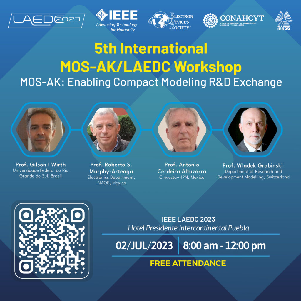
MOS-AK WORKSHOP
MOS-AK: Enabling Compact Modeling R&D Exchange
In-person sessions will take place at the Intercontinental Hotel in Puebla.
Date: July 2, 2023.

Synopsis:
- HiTech forum to discuss the frontiers of electron device modeling with emphasis on simulation-aware compact/SPICE models and its Verilog-A standardization.
- MOS-AK Meetings are organized with aims to strengthen a network and discussion forum among experts in the field, enhance open platform for information exchange related to compact/Spice modeling and Verilog-A standardization, bring people in the compact modeling field together, as well as obtain feedback from technology developers, circuit designers, and CAD tool vendors. The topics cover all important aspects of compact model development, implementation, deployment and standardization within the main theme – frontiers of the compact modeling for nm-scale MEMS/NEMS designs, CMOS/SOI and HEMT IC simulation.
- The specific workshop goal will be to classify the most important directions for the future development of the electron device models, not limiting the discussion to compact models, but including physical, analytical and numerical models, to clearly identify areas that need further research and possible contact points between the different modeling domains. This workshop is designed for device process engineers (CMOS, SOI, BiCMOS, SiGe, GaN, InP) who are interested in device modeling; ICs designers (RF/Analog/Mixed-Signal/SoC/Bio/Med) and those starting in that area as well as device characterization, modeling and parameter extraction engineers. The content will be beneficial for anyone who needs to learn what is really behind the IC simulation in modern device models in particular using free open source PDKs.
Workshop Topics:
- Advances in semiconductor technologies and processing
- Compact Modeling (CM) of the electron devices
- Verilog-A language for CM standardization
- New CM techniques and extraction software
- Open Source FOSS TCAD/EDA modeling and simulation
- CM of passive, active, sensors and actuators
- Emerging Devices, CMOS and SOI-based memory cells
- Microwave, mmW, RF device modeling, high voltage device modeling
- Microsystems, SoC, IP modeling
- Device level modeling for Bio/Med applications
- Nanoscale semiconductor devices/circuits and its reliability/ageing
- Technology R&D, DFY, DFT and IC Designs
- Foundry/Fabless Interface Strategies (eg: Skywater 130nm CMOS free PDK)

Prof. Gilson I Wirth
UFRGS – Universidade Federal do Rio Grande do Sul
Departamento de Engenharia Eletrica
Av. Osvaldo Aranha, 103
90035-190 – Porto Alegre – RS
Brazil
Charge Trapping in Semiconductor Devices: From Device Level Modeling to Circuit Analysis
Prof. Gilson I Wirth
BIOGRAPHY:
Gilson Wirth received the B.S.E.E and M.Sc. degrees from the Universidade Federal do Rio Grande do Sul, Brazil, in 1990 and 1994, respectively. In 1999 he received the Dr.-Ing. degree in Electrical Engineering from the University of Dortmund, Dortmund, Germany.
He is currently a professor at the Electrical Eng. Depart. at Univ. Federal do Rio Grande do Sul – UFRGS (since January 2007).
From July 2002 to December 2006 he was professor and head of the Computer Engineering Department, Univ. Estadual do Rio Grande do Sul – UERGS.
His current research work focuses on modeling and electrical stimulation of charge trapping in the context of Bias Temperature Instability (BTI), Low-Frequency Noise (1/f and RTN) and Hot Carrier Degradation (HCD).
He has also worked on ionizing radiation effects (TID and SET/SEU) on semiconductor devices.
He focuses on collaborative work with academia and industry. He has stablished successful collaborative work with different companies and research groups in Europe, North and South America, and China. Has signed NDA with the following companies: Intel, Texas Instruments, NXP Semiconductors and Infineon Technologies.
He is currently a Distinguished Lecturer of the IEEE Electron Devices Society. He also was a distinguished lecturer of the IEEE Circuits and Systems Society (term 2010-2011).
An updated list of publications may be found at http://lattes.cnpq.br/1745194055679908
Or https://www.webofscience.com/wos/author/record/319677
Or https://www.scopus.com/authid/detail.uri?authorId=8700162500
Abstract: Benchmarking metrics for circuits based on Field Effect Transistors are discussed. The basics mechanisms involved in charge trapping are presented. Modeling techniques to abstract the physical level effects into the circuits design flow are studied. Charge trapping leads to noise and aging (BTI). Noise levels and BTI degradation can vary by several orders of magnitude in deeply scaled devices, making variability a major concern in advanced MOS technologies. Therefore, to assure proper circuit design in this scenario, it is necessary to identify the fundamental mechanisms responsible for variability of noise and BTI. The applicability of the model here presented to the evaluation of integrated circuits in both time and frequency domain is discussed.

Prof. Roberto S. Murphy Arteaga
Chair of the Electronics Department
INAOE
Second order aspects of characteristic impedance determination
Prof. Roberto S. Murphy-Arteaga
BIOGRAPHY:
Roberto S. Murphy-Arteaga received his B.Sc. degree in Physics from St. John’s University, Minnesota, and got his M.Sc. and Ph.D. degrees from the National Institute for Research on Astrophysics, Optics and Electronics (INAOE), in Tonantzintla, Puebla, México. He has been a researcher at INAOE since 1988. Since then, he has presented over 140 talks at scientific conferences, directed twelve Ph.D. dissertations, 19 M.Sc. and 3 B.Sc. theses, published more than 160 articles in scientific journals, conference proceedings and newspapers, and is the author of a text book on Electromagnetic Theory. His research interests are the physics, modeling and characterization of the MOS Transistor and passive components for high frequency applications, especially for CMOS wireless circuits, as well as antenna design for wireless communications.
He is a member of the Mexican Academy of Sciences, of the Mexican National
System of Researchers (SNI), as well as a Distinguished Lecturer of IEEE-EDS.
Abstract: : In this talk, the characteristic impedance (Zc) extraction from experimental data is explored. Different problems in the Zc vs frequency (f) curves (associated with the adapters used to access the lines) are exposed, such as a different level of Zc with respect to the expected value, and resonances due not only to signal reflections in the transmission line structure, but also along the adapter length. Ad hoc structures were used to analyze the effects of connectors, needed to probe transmission lines, both on-chip and on printed circuit boards (PCBs)

Prof. Antonio Cerdeira Altuzarra
Cinvestav-IPN (MX)
Distinguished Lecturer IEEE EDS
Current Dependence on Temperature in FinFETs, Nanowires, Nanosheets and stacked MOS devices.
Prof. Antonio Cerdeira Altuzarra
BIOGRAPHY:
He received the M.Sc. degree in physics from Moscow State University, Russia, in 1966 and the Ph.D. degree from the NW Leningrad Polytechnic Institute, Russia, in 1977. Since 1966, he has been engaged in research, teaching and development in the field of microelectronics, including design, technology, characterization, simulation and modeling. He has been Professor at the Faculty of Physics, 1966-1979 and Director of the Solid-State Electronics Research Laboratory, 1968-1979, both at University of Havana; head of Research Department at National Institute of Automatized System (INSAC) in Havana, Cuba, 1979-1990; from 1990-1994 head of Microelectronic Department at International Center of Informatics in Moscow and since 1995 he is a Full Professor at the Section of Solid-State Electronics, Department of Electrical Engineering, Center of Research and Advanced Studies (CINVESTAV) in México City. He has also been head of 14 research and infrastructure projects; author, coauthor of more than 300 technical papers and 4 patents. His actual research interest is in the field of modeling and characterization of multigate nanometric MOSFETs and Thin-Film Transistors (TFT), including the non-linear behavior of devices and circuits. Prof. Cerdeira is a Life Senior Member of the IEEE and IEEE Electron Devices Society Distinguished Lecturer.
The current scaling of MOSFETs towards sub-20 nm long devices is being sustained by adopting devices using multiple gate (MuGFETs) architectures. Amongst the MuGFETs, the FinFETs achieved maturity for mass production. FinFETs are made with tall and narrow silicon fins. For the scaling of FinFETs, nanowire MOS transistors (or simply nanowire transistors) emerged as an excellent alternative. Nanowire transistors are FinFET-like structures consisting of three gates, with the transistor Fin height (HFIN) having a similar dimension as Fin width (WFIN). If the device has a WFIN wider than HFIN and the gate surrounds the silicon region this transistor is referred as nanosheet transistor. When more than one transistor is placed over other, a stacked structure is obtained.
Recently, a compact model developed for FinFETs, the Symmetric Doped Double-Gate Model (SDDGM) was complemented and validated for modelling the drain current of nanowire and nanosheet transistors. However, the modelling of nanowires, nanosheet and stacked MOS devices at high temperatures was missing. Recently, we analysed the possibility of using the expressions in the SDDGM, that include all temperature-dependent factors, for modelling nanowire, nanosheets and staked MOS devices with temperature.
Additionally, the leakage current as function of temperature was analysed for nanowires, which include the tunnelling currents and an additional current component of P-N junction Source-Channel, that was not previously considered. The drain current, considering the above-mentioned leakage currents, is then calculated as function of temperature.
In this presentation, we show the modelling of nanowires, nanosheet and stacked MOS with temperature. The modelling of nanowires, including all components of the leakage current, also as function of temperature, is also presented. All results are validated with experiment.

Léopold Van Brandt, PhD
research fellow in the
Mathematical Engineering department of the UCLouvain
Variability and Intrinsic Noise Effects in ULV CMOS SRAM Demystified
Léopold Van Brandt, PhD
BIOGRAPHY:
Léopold Van Brandt was born in Belgium, in 1995. He received the B.S. and the M.S. degrees in Electrical Engineering from the Université catholique de Louvain, Louvain-laNeuve, in 2015 and 2017, respectively, and the PhD degree in Engineering Science for his dissertation entitled “Statistical Analyses of Intrinsic Noise and Variability Effects in CMOS Digital Latches” in 2022. He is currently working as a postdoctoral research fellow in the Mathematical Engineering department of the UCLouvain on the project “Thermodynamics of Circuits for Computation”.
His research interests include but are not limited to: nanoelectronics; characterization and modelling of the noise in nonlinear devices and circuits; circuit simulation theory; efficient assessment of the reliability of SRAM bitcells; stochastic thermodynamics. The interplay between research and education is one of his major concerns.
Since each Static Random Access Memory (SRAM) array typically contains hundreds of thousands of bitcells (e.g. 262 144 for 32 kB), a cell failure probability as low as the ppm must be guaranteed for a given design across various process, voltage and temperature conditions.
The MOS transistors of smallest dimensions and supplied at ultra-low voltage (ULV) are very sensitive to all types of uncertainties. As process variability has remained the major concern for now, we will firstly introduce an insightful and accurate non-Monte Carlo methodology to predict the variability-induced failure probability of subthreshold SRAM bitcells in retention mode. Secondly, the intrinsic noise of the MOS transistors, especially experimentally-reported large-amplitude random telegraph noise (RTN), is likely to induce transient bit flips in bitcells weakened by worsened voltage, temperature and process variability conditions. Because the
noise cannot be studied within a purely static formalism, we propose a rigorous simulation framework, relying on industrial SPICE tools and process design kits (PDK), to observe and explain these bit flips. Finally, extending the reliability perspective, we will conclude this talk by quantitatively discussing the relative impact of process variability, RTN and Gaussian noise in mature industrial CMOS technology such as 28nm FD SOI