IEEE EDS R9 Summer School
Design, Characterization, and Reliability of Sensors and Integrated Circuits
Description
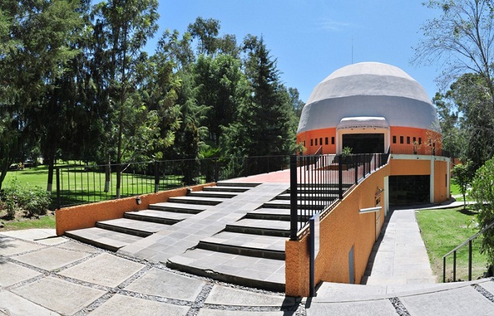
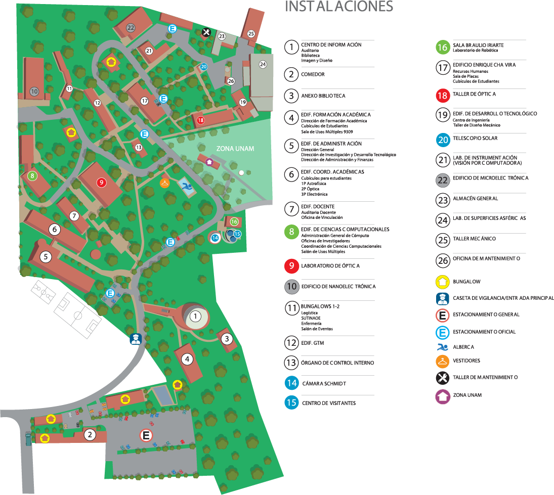
The summer course is going to be hosted by the National Institute for Astrophysics, Optics and Electronics (INAOE) and organized by the 2022 IEEE Latin American Conference LAEDC from 1-3 July 2022 in Puebla, Mexico. This will be a three-day workshop including lectures, guided laboratories tours, experiments, hands-on training and research experience in the design, fabrication and testing of integrated circuits (IC) fabricated in Latin America.
This summer school will include.
- Scholarship opportunities for selected participants including registration, lodging and meals
- Virtual presentations for remote participants
- Certificate of participation
APPLICATION DEADLINE: |
|
|---|---|
Thursday, June 30 2022 (For Virtual participants). |
Agenda Overview
An overview of the IEEE EDS R9 Summer School 2022 on design, characterization, and reliability o sensors and integrated circuits agenda can be seen below. This agenda will be updated as more events are finalized.
FIRST DAY FRIDAY JULY 1: Semiconductor materials, devices, and fabrication
MORNING
| Time | Speaker | Title |
|---|---|---|
| 08:00 - 09:00 | REGISTRATION | |
| 08:30 - 09:30 | Fernando Guarin | Opening remarks and overview of the semiconductor industry |
| 09:30 - 10:30 | Edmundo Gutiérrez | Introduction to semiconductor materials and device physics |
| 10:30-10:50 | COFFEE BREAK | |
| 11:00-12:30 | Alfonso Torres | Semiconductor device fabrication process |
AFTERNOON
| Time | Speaker | Title |
|---|---|---|
| 12:30-14:00 | LUNCH | |
| 14:00-15:30 | Alba Avila | Practical aspects of clean room and operation |
| 15:30-16:00 | Virtual tour | Virtual tour to the 0.8 µm INAOE fabrication lab. |
SECOND DAY SATURDAY JULY 2: Design and applications
MORNING
| Time | Speaker | Title |
|---|---|---|
| 9:00-10:30 | Edmundo Gutiérrez | Cryogenic operation of semiconductor devices |
| 10:30-10:50 | COFFEE BREAK | |
| 10:50-12:30 | Elkim Roa | Digital Design: From transistors to computing |
AFTERNOON
| Time | Speaker | Title |
|---|---|---|
| 12:30-14:00 | LUNCH | |
| 14:00-15:00 | Maria Teresa Sanz | Design of analog integrated circuits |
| 15:00-16:00 | Claudia Reyes | Design and fabrication of bio-chemical sensors |
| 16:00-16:20 | COFFEE BREAK | |
| 16:20-17:20 | Alejandro Bautista | Overview of the first Latin-American IC Design Contest |
THIRD DAY SUNDAY JULY 3: Systems, characterization, and reliability
MORNING
| Time | Speaker | Title |
|---|---|---|
| 9:00-10:30 | Daniel Durini | Radiation sensors, theory and practice |
| 10:30-10:50 | COFFEE BREAK | |
| 10:50-12:40 | Fernando Guarin | Semiconductor Reliability Overview including RF/mmW/5G |
AFTERNOON
| Time | Speaker | Title |
|---|---|---|
| 12:30-14:00 | LUNCH | |
| 14:00-15:30 | Wilfrido Moreno | Model-Based Systems Engineering (MBSE) |
| 15:30-16:00 | CERTIFICATES OF PARTICIPATION | |
Speakers

Biography
Claudia Reyes-Betanzo is a researcher in the Electronics Department at the National Institute for Astrophysics, Optics, and Electronics (INAOE) in Puebla, Mexico, since 2003. She received the M.Sc. degree in Semiconductor Devices from the Autonomous University of Puebla, and the Ph.D. degree in Microelectronics from the State University of Campinas, Brazil, in 2003. Her current research interests include biosensor, flow sensors, and micro fluidic systems.
Course. Design and fabrication of bio-chemical sensors
The state of the art in biosensors and the specific study of electrochemical-based biosensors will be presented in this short course, focusing in detection principles, figures of merit, requirements, applications, and challenges. Finally, the currently progress of the design, and fabrication of an impedimetric biosensor of interdigitated electrodes for detection of Escherichia coli (E.coli) carried out in INAOE will be shown.
Biography
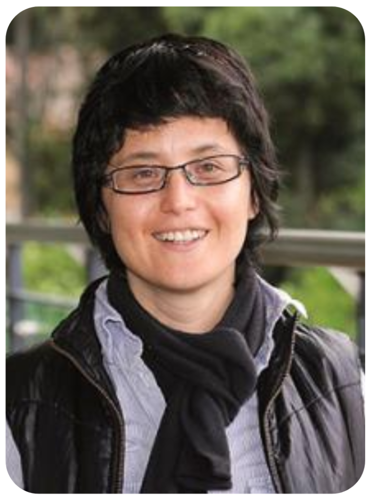
Dr. Alba Avila is an Associate Professor at the Electrical and Electronic Department of the University of Los Andes where she has been a faculty since 2003. She holds a Ph.D. in Physics from the University of Cambridge in the U.K., a Masters in Electrical Engineering and a B.A. in Physics and Electrical Engineering from the University of Los Andes. Her areas of expertise include electrical characterization of materials using microscopy techniques, new physco-chemical techniques for toxicity assessment, remote sensing of water and integrating nanomaterials in the field of sustainability. She also works on designing and developing electronic kits to promote nanotechnology education and engages regularly in outreach activities with marginalized communities. She was the researcher leader for the set up of the first cleaning room in Colombia.
Course. Practical aspects of clean room and operation
The talk describe the practical aspects of the design, running, and maintenance of a clean room in Latin America. These include the training of human resources not always available in the region, and the training on procedures, processes, and safety. I discuss the need to assess the performance of equipment at high altitudes, a characteristic in our region. In addition to regulation of controlled chemicals (generally related to precursor chemicals) and their Rigorous monitoring of acquisition, use, and waste. We will discuss what are the pertinent metrics to measure the impact of having access to a clean room at Uniandes? Metrics vs key performance metrics (KPIs)? Shall we register the statistics of users and active projects or instead the products/ the researcher’s density? There is a need to expose undergraduate students to semiconductor and sensor fabrication processes within the vision of educational training and delivering products that could be patented, registered, and use by businesses and entrepreneurs, and startups. Not always clean room generating profitable indicators special impacted with the high maintenance cost on top of the consumable inflated prices but an educational training space that has to be supported with the vision of having a space to allow the students to develop skills for the fabrication and testing of devices on which further learning could build in their life-long learning journeys.
The talk will highlight the differences based on the geographical location and the types of operations undertaken in the cleanrooms and the need for a collaborative alliance that will strengthen our capacities by creating an inventory of the region’s capacities and a network of cleanrooms that will allow students to be exposed to a larger chain of semiconductor and sensors process.
Biography
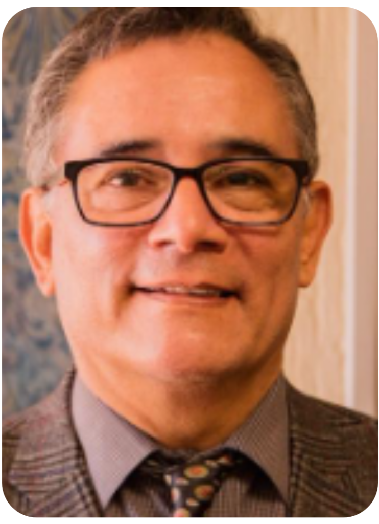
Dr. Edmundo A. Gutiérrez-D. received the PhD from the Catholic University of Leuven, Belgium in 1993, with the thesis entitled “Electrical performance of submicron CMOS technologies from 300 K down to 4.2K”. From 1988 to 1993 was a research assistant at the Interuniversity Microelectronics Center (IMEC) in Leuven, Belgium. In 1993 joined as a researcher the Department of Electronics of INAOE. In 1996 spent one year as invited Professor at the Simon Fraser University in Vancouver, Canada. In 1996 he also spent two months at the University of Sao Paulo, Brazil as a Summer PhD lecturer. From 1999 to 2000 was appointed Head of the INAOE Department of Electronics. From 2000 to 2002 spent two years as Design Manager of the Motorola Mexico Center for Semiconductor Technology in Puebla City. In 2002 he was also invited Professor at the Technical University of Vienna, Austria. From 2002 to 2005 rejoined INAOE as Professor of the Department of Electronics. From 2005 to 2007 was the Research Manager of the Intel Systems Research Center Mexico in Guadalajara City.
Prof. Gutiérrez is author of the book “Low Temperature Electronics, Physics, Devices, Circuits and Applications” (Academic Press, 2000), and the book “Nano-Scaled Semiconductor Devices, Physics, Modelling, Characterisation, and Societal Impact” (IET Press, 2016). He has supervised 4 M.Sc. and 15 PhD theses and has published more than 140 scientific papers and conferences in the field of physics of semiconductor materials and devices, including MOS transistors, temperature, optical, and magnetic sensors. He is Editor-In-Chief of the IEEE Transactions on Devices and Materials Reliability journal.
Currently Prof. Gutierrez is the General Director of the National Institute of Astrophysics, Optics and Electronics (INAOE) in Puebla, Mexico. Prof. Gutiérrez is an IEEE Fellow.
Course. Cryogenic operation of semiconductor devices
The temperature dependence of the physical properties of semiconductor materials, and the electrical performance of electron devices, is reviewed in this introductory course. The full range from 300 Kelvin degrees (300 K) down to and below 1 K is covered. Special attention is paid to temperatures around liquid helium (4.2 K) and below, where the materials and devices enters the “energy freeze-out regime”. This “freeze-out” regime is of interest for quantum devices and quantum computing, as well as several types of sensors used in medicine and scientific instruments.
Course. Introduction to semiconductor materials and device physics
This is an introductory course that describes the physical properties of various semiconductor materials used in the fabrication of electron devices. This covers the most widely useful and interesting properties, such as energy distribution, carrier density, carrier mobility, electrical conductivity, thermal resistance, and capacitance. Other interesting properties related to the sensitivity to magnetic or mechanical signals, are also covered. The interaction of a semiconductor surface with biological and chemical species is also succinctly reviewed, as it is of relevance for the design and fabrication of bio-chemical sensors. The use of various semiconductor materials in the design and fabrication of Metal-Oxide-Semiconductor Field Effect Transistors (MOSFET) and sensors is explained. Finally, a brief review on the physics behind of the operation of MOSFETs and sensors is introduced.
Biography
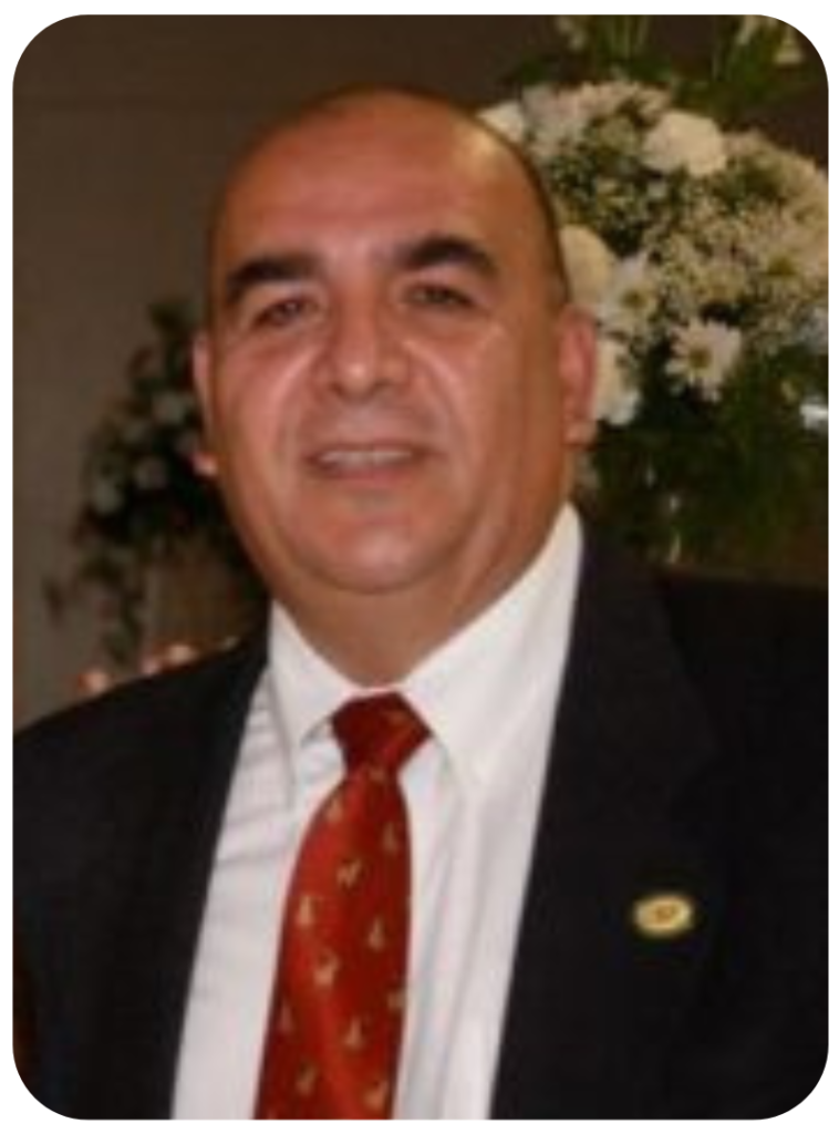
Wilfrido Moreno received his M.S.E.E & Ph.D. degrees in Electrical Engineering from the University of South Florida (USF), Tampa – Florida in 1985 and 1993 respectively. He is currently a Professor in the Electrical Engineering Department at the University of South Florida, Tampa – Florida. Since 1994, Dr. Moreno has been facilitating students and faculty mobility throughout the Latin American region; over 120 faculty members have earned their Doctoral degrees from USF. From 2003, Dr. Moreno has served as the R&D Initiative Director for the Ibero-American Science & Technology Education Consortium (ISTEC) responsible for fostering Teaching/Learning & Research collaborations throughout the Ibero-american region among ISTEC’s members. Dr. Moreno is a founding member of the former Center for Microelectronics Research, (CMR- 1988), which is currently the Nanotechnology Research & Education Center, (NREC). Dr. Moreno is the author of over 130 technical publications. His research interests are oriented toward system integration by providing hardware/software solutions to industrial applications in areas such as Digital Signal Processing, Communications, Energy, Robotics & Control, Nano/Micro-electronics, Medical Engineering and Multimedia solutions applied to engineering education. Dr. Moreno has supervised over sixty master students and twenty-three doctoral students.
Course. Model-Based Systems Engineering (MBSE)
Model-Based Systems Engineering (MBSE) is the formalized application of System Modeling to support Agile System of Systems Engineering, which is a methodical, disciplined approach for the design, realization, technical management, operations, and implementation of a system, i.e., single system, complex system, system of systems, Digital Twins, etc. Methodologies based on the System of Systems Engineering approach to solve complex engineering applications driven by Digital Engineering trends will be presented. In this course, main concepts about the process of Systems Engineering (SE), and how can is applied to different situations or needs (like semiconductor manufacturing) and what models, techniques, methods, formats, and standards are available today. This course will also include selected topics within Cybersecurity, Digital Twins where MBSE methodologies are already used to realize and demonstrate the utilization of various analytical models and methods for accomplishing system analysis and design, not only in the design and evaluation of new systems, but in the evaluation and design applied to existing systems for the purpose of their improvement. Also emphasized is the need to properly integrate a variety of engineering design and management disciplines to effectively implement the concepts and principles of Model Based Systems Engineering including modern industry tools for architecture, design, development, verification, validation, and life cycle management using agile or waterfall approaches.
Biography
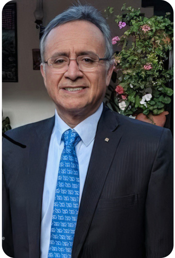
Dr. Fernando Guarín is a Distinguished Member of Technical Staff at Global Foundries in East Fishkill New York. He retired from IBM’s SRDC after 27 years as Senior Member of Technical Staff. He earned his BSEE from the “Pontificia Universidad Javeriana”, in Bogotá, Colombia, the M.S.E.E. degree from the University of Arizona, and the Ph.D. in Electrical Engineering from Columbia University, NY He has been actively working in microelectronic reliability for over 40 years.
From 1980 until 1988 he worked in the Military and Aerospace Operations division of National Semiconductor Corporation. In 1988 he joined IBM’s microelectronics division where he worked in the reliability physics and modeling of Advanced Bipolar, CMOS and Silicon Germanium BiCMOS technologies. He is currently leading the team qualifying GlobalFoundries RF 5G technology offerings.
Course. Introduction to the Semiconductor Industry
In this course we will introduce students the economics and driving forces influencing the global semiconductor industry. We will explain the roles of Pure-play semiconductor foundries as well as those of Integrated device manufacturers (IDMs). The role of scaling and innovation will be presented and analyzed. We will cover the evolution of the industry from both, the materials and device implementation perspectives. The course will also review the roadblocks and challenges solved over the last few decades and cover relevant topics dealing with the state of the art and the path forward for the near and long-term. We will finish the course with some thoughts about the importance of the semiconductor industry and its geopolitical implications emphasizing the importance for the Latin-American region.
Course. Semiconductor Reliability Overview including RF/mmW/5G
In this course we will provide a comprehensive review of the major reliability mechanisms and relevant semiconductor reliability methods and modeling approaches that are widely accepted and used by industry. We will start with a general introduction and then will cover the major Front End OF Line (FEOL) mechanisms; Hot Carriers (HC), Time Dependent Dielectric Breakdown (TDDB), Bias Temperature Instability (BTI). We will then cover the major Back End Of Line (BEOL) Reliability mechanisms; Electromigration EM, Stress Migration SM, Thermal Cycling (TC), Time Dependent Dielectric Breakdown (TDDB) and then we will review the Middle Of the Line (MOL) Reliability mechanisms. We will provide an overview of Self Heating.
Up to this point in the evolution of leading-edge Silicon CMOS technologies the qualification of the latest nodes has been carried out using the methods and targets dictated by digital/logic applications. For RF applications the digital centric methodology and metrics will no longer be applicable. We will discuss the reliability impact of miniaturization and the qualification activities driven by the need to support reliable operation for RF circuit applications. The CMOS solutions for RF applications include the introduction of SOI that may introduce additional reliability considerations. The path to maintaining the advanced CMOS scaling cadence and new reliability limiting factors will be examined from the reliability perspective. We will also review the reliability requirements for RF reliability devices and applications as we prepare to introduce technologies to serve the 5G infrastructure requirements. A closer look will be given to Hot Carriers. The characterization, models and qualification methodologies will be put in the required perspective for the successful qualification and transfer of leading edge technologies to a manufacturing environment.
Biography
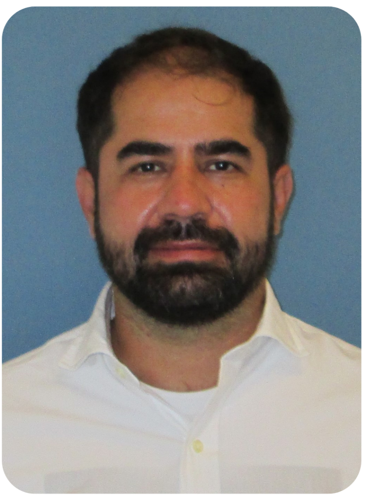
Elkim received his Ph.D. degree in electrical and computer engineering from Purdue University, where he was a Fulbright Scholar, his Master’s degree from the University of São Paulo, São Paulo, Brazil, and his bachelor’s degree in Electrical Engineering from Universidad Industrial de Santander, Colombia. From 2014 to 2016, he was with Rambus, Inc., where he was engaged in high-speed SERDES front-end design. From 2016 to 2021 he was an Associate Professor at Universidad Industrial de Santander. Currently, he is a system architect at Globalfoundries, Santa Clara, CA. His research interests include circuits and architecture design for security, front-end circuits for high-speed interfaces, and low-energy and efficient computing.
Course. Digital Design: From transistors to computing
This short tutorial will give a bird view of the tools and methodology to build digital compiled silicon. The first half of the tutorial will focus on how to build a standard cell library. The second half of the tutorial will focus on the synthesis, placement, and routing of RISC-V-based processors.
Biography
Daniel Durini is currently Research and Development Director and a full Research Professor in areas of microelectronics and radiation detection at the National Institute of Astrophysics, Optics and Electronics (INAOE) in Puebla, Mexico. He obtained the B.Sc. degree in Electrical-Electronic Engineering from the National Autonomous University of Mexico (UNAM) in 2002, the M.Sc. degree in area of Microelectronics from the National Institute of Astrophysics, Optics and Electronics in Mexico in 2003, and the Ph.D. degree in area of Microelectronics from the University of Duisburg-Essen in Germany in 2009. He was with the Fraunhofer Institute for Microelectronic Circuits and Systems (IMS) in Duisburg, Germany, between 2004 and end of 2013, where he led during the last four years a group dedicated to developing special CMOS process modules for high-performance photodetection devices, pixel structures and imagers.

Biography
Received the degree of Doctor in Sciences in Electronics from the INAOE. The M. Sc. Degree from University of New Mexico in Electrical Engineering, and the Chemical Engineering degree form Universidad Autónoma de Puebla. Currently is a Researcher in the Electronics Department at INAOE, his research interest are physics and technology of semiconductor devices, deposition and characterization of Nano structured materials.
Course. Semiconductor device fabrication process
Silicon device fabrication process may be seen as a sequence of alternating a photolithographic process and a thermal treatment. In this tutorial, the fabrication process for integrated circuits in a CMOS technology with sub-micron features will be described. Also, the critical fabrication steps will be underlined and the evolution towards Nano metric devices will be displayed.


