Mini Colloquium
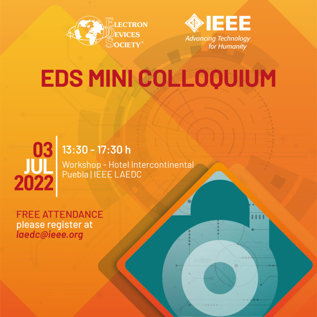
In-person sessions will take place at the Intercontinental Hotel in Puebla. Máximo Serdán room.

Speakers

Biography
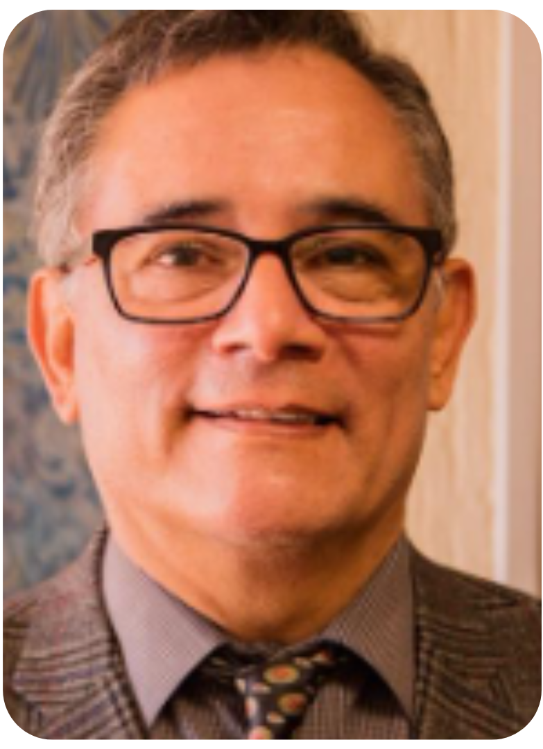
Prof. Lluis F. Marsal is Distinguished Professor and full professor at the University Rovira i Virgili, Spain. Ph.D. from the University Politecnica de Cataluña, Spain, 1997. Postdoctoral researcher at the ECE, University of Waterloo, Canada (1998-1999).
In 2012, he received the URV’s RQR Award for the high quality in research and in 2014, he received the UniSA Distinguished Researcher Award, and the 2014 and 2021 ICREA Academia Awards from the Generalitat of Catalunya. Since 2019, he is the Chair of the Subcommittee for Regions/Chapters (SRC) – Regions 8 IEEE- EDS and member of the Regions & Chapters Committee and Member of the EDS Technical Committee on Photovoltaic Devices. He is a senior member of the IEEE and a member of the Distinguished Lecturer program of the EDS. He is also an Optica Fellow (formerly OSA) for his leading contributions to optoelectronic and sensing devices and photonic and optical nanostructured materials. He has been a member of advisory and technical committees in several international and national conferences and has been visiting professor at several universities and research institutions (CINVESTAV – Instituto Politécnico Nacional, Mexico, McMaster University, Canada, ICMM-CSIC, BiomaGUNE, Spain, Mawson Institute, Australia). He has co-authored more than 200 publications in international refereed journals, 2 books, 5 book chapters and 4 patents. His current research interests focus on polymer and hybrid solar cells and nanostructured materials for optoelectronic devices and low–cost technologies based on micro- and nanoporous materials for biosensing and bio-applications.
Abstract
Organic solar cells are considered as a promising renewable energy source because of their light-weight, high transparency, possibility of fabrication in large areas and inexpensive solar energy production. These solar cells are based in the junction of two different organic semiconducting materials, one donor and one acceptor. The most efficient devices to date are the bulk heterojunction cells, obtained from a mixture of the donor and acceptor materials, which provides an enormous interfacial surface.
In the last years, advances in polymer-based organic solar cells have been possible due to different approaches such as design of new structures and synthesis of new materials such as small molecule and polymers with low band-gaps, control of the nanoscale morphology, new interfacial transport layers, variation of the ratio of the donor/acceptor in the bulk heterojunction, application of thermal or solvent annealing process, among others [1-4]. As a result, recently, power conversion efficiencies over 18% are obtained [5]. However, there are still room for improving and some problems should be solved such as the stability, and degradation process of the polymer solar cells [6-7]. In this lecture, we will present the perspectives and recent advances made in polymer solar cells, design and synthesis of new polymers and in particular the active layer morphology, interfacial layers and stability. We will also discuss the basic device operation and various parameters limiting their efficiency and their possible improvements.

Biography
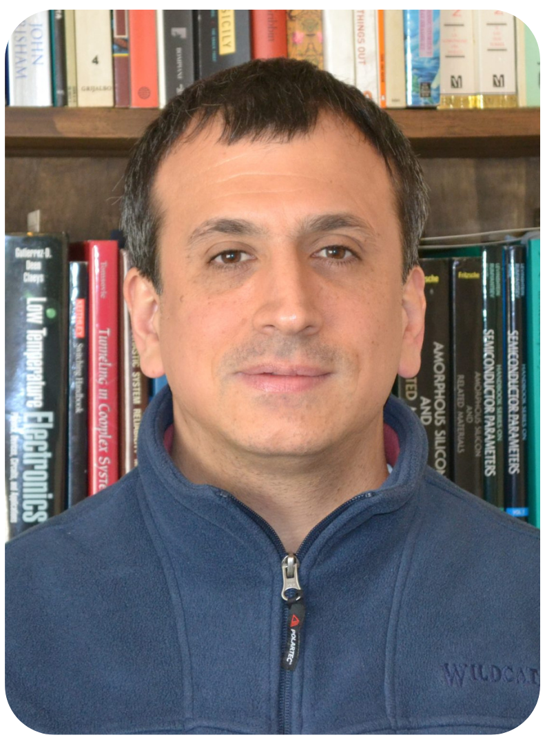
Dr. Edmundo A. Gutiérrez-D. received the PhD from the Catholic University of Leuven, Belgium in 1993, with the thesis entitled “Electrical performance of submicron CMOS technologies from 300 K down to 4.2K”. From 1988 to 1993 was a research assistant at the Interuniversity Microelectronics Center (IMEC) in Leuven, Belgium. In 1993 joined as a researcher the Department of Electronics of INAOE. In 1996 spent one year as invited Professor at the Simon Fraser University in Vancouver, Canada. In 1996 he also spent two months at the University of Sao Paulo, Brazil as a Summer PhD lecturer. From 1999 to 2000 was appointed Head of the INAOE Department of Electronics. From 2000 to 2002 spent two years as Design Manager of the Motorola Mexico Center for Semiconductor Technology in Puebla City. In 2002 he was also invited Professor at the Technical University of Vienna, Austria. From 2002 to 2005 rejoined INAOE as Professor of the Department of Electronics. From 2005 to 2007 was the Research Manager of the Intel Systems Research Center Mexico in Guadalajara City.
Prof. Gutiérrez is author of the book “Low Temperature Electronics, Physics, Devices, Circuits and Applications” (Academic Press, 2000), and the book “Nano-Scaled Semiconductor Devices, Physics, Modelling, Characterisation, and Societal Impact” (IET Press, 2016). He has supervised 4 M.Sc. and 15 PhD theses and has published more than 140 scientific papers and conferences in the field of physics of semiconductor materials and devices, including MOS transistors, temperature, optical, and magnetic sensors. He is Editor-In-Chief of the IEEE Transactions on Devices and Materials Reliability journal.
Currently Prof. Gutierrez is the General Director of the National Institute of Astrophysics, Optics and Electronics (INAOE) in Puebla, Mexico. Prof. Gutiérrez is an IEEE Fellow.
Abstract
Although computing requires cryogenic temperatures to operate properly, these days it has become a hot topic, so special attention is required. In this talk I will focus on talking about CMOS technology, and its operation at cryogenic temperatures (4.2 K and below). Various CMOS technologies are being considered for potential use as control and reading systems for in-situ Qubits. That is, the possibility of placing the electronics as close as possible to the Qubits array. However, for this to be possible it is necessary to analyze energy efficiency and electro-thermal coupling.

Biography
Subramanian S. Iyer (Subu) is Distinguished Professor and holds the Charles P. Reames Endowed Chair in the Electrical Engineering Department and a joint appointment in the Materials Science and Engineering Department at the University of California at Los Angeles. He is Director of the Center for Heterogeneous Integration and Performance Scaling (UCLA CHIPS). Prior to that he was an IBM Fellow. His key technical contributions have been the development of the world’s first SiGe base HBT, Salicide, electrical fuses, embedded DRAM and 45nm technology node used to make the first generation of truly low power portable devices as well as the first commercial interposer and 3D integrated products. He also was among the first to commercialize bonded SOI for CMOS applications through a start-up called SiBond LLC. More recently, he has been exploring new packaging paradigms and device innovations that may enable wafer-scale architectures, in-memory analog compute and medical engineering applications. He has published over 300 papers and holds over 75 patents. He has received several outstanding technical achievements and corporate awards at IBM. He is an IEEE Fellow, an APS Fellow, an iMAPS Fellow and a Distinguished Lecturer of the IEEE EDS and EPS and a member of the Board of Governors of IEEE EPS. He is also a Fellow of the National Academy of Inventors. He is a Distinguished Alumnus of IIT Bombay and received the IEEE Daniel Noble Medal for emerging technologies in 2012 and the 2020 iMAPS Daniel C. Hughes Jr Memorial award and the iMAPS distinguished educator award in 2021.
Abstract
Machine learning and Inference are a significant portion of modern computing. Using conventional processors and accelerators including CPUs, GPUs, and custom ASICs, this computing is very memory intensive with frequent calls to memory which are extremely power hungry. Since the discovery of the memristor, there has been a resurgent interest in analog in-memory compute. Most often, this takes the form of a 1T-1R cell in a cross-point architecture. At UCLA CHIPS, we have been investigating the use of classical CMOS on SOI device used in a somewhat unconventional way. We call this device the Charge Trap Transistor and it’s a regular SOI NFET device whose threshold voltage can be controllably and reversibly changed by self-heating assisted trapping in the HiK dielectric. The device is operated in the subthreshold and a small change in the subthreshold voltage can cause a large change in the sub-threshold drain current. We can show 1000X dynamic range with an effective bit resolution of as much as 5-6 bits. In this talk, we will describe this work, including programming schemes, temperature stability and simple MAC (multiply and accumulate) operations. The CTT is a robust device for in-memory analog compute and promises to enable a viable and resilient edge-based inference engine especially for embedded and IoT applications.

Biography
Felix Palumbo has received the MSc. (2000) and Ph.D. (2005) both in physics from the University of Buenos Aires, Argentina. He is an active researcher in the field of semiconductor device physics and reliability, with experience in the academy and industry (Tower Jazz- Israel) well embedded within international research collaboration. In 2012–2014, he was Marie Curie postdoctoral fellow at Technion Institute Israel, in the 2015 IEEE-IRPS edition, he has been invited to present a review talk on CMOS Reliability, and in 2019 he was awarded by the IEEE-IRPS as the Best Paper.
At present, he is a research staff of the National Council of Science and Technology(CONICET), and a full professor at National Technological University (UTN) in Buenos Aires, Argentina. He is a reviewer of several scientific journals, author of 3 review articles, and of about 80 scientific and technical papers published in international peer-reviewed journals and conferences. His current research interests include electronic device reliability, breakdown effects of ultra-thin dielectrics, radiation effects, and the early assessment of emerging technologies.
Abstract
Thin dielectrics are the fundamental stone over which semiconductor industry experienced its huge development. As the key element for manufacturing Metal Oxide Semiconductor Field Effect Transistors, guaranteeing the reliability of gate oxides has become more challenging with the pushing demands of the markets for improved performance in electronic devices. In this framework, understanding not only the statistics but the physical phenomena behind dielectric breakdown is crucial to ensure the reliability of modern and future electronic devices. In this lecture, the fundamentals of thin dielectric breakdown and the state of the art of breakdown studies on novel materials is summarized, focusing on the physical phenomena that characterize thin film dielectric breakdown and the perspectives on novel 2D materials, that demonstrate remarkable potential to be applied as gate insulators in future nano-electronic devices.


