Kenote Speakers

Abstract
184 years ago, in 1838, ‘relay’ — the first digital signal amplifier — provided us with the long-distance telegraph through electric wires. This is the beginning of the information society and ‘electrical engineering’ era. 116 years ago, in 1906, ‘triode vacuum tube’ — the first analog/digital signal amplifier — brought us ‘electronics’ that can manipulate the electron movement, as we wish, for use for wireless-telecommunication and machine-control. 75 years ago, in December 1947, the ‘transistor’ was invented as the first solid-state amplifier for the purpose of device-size reduction in order to realize high-frequency and low-power operation. This is the origin of the device miniaturization for micro/nanoelectronics. The 10 millionths-times device-size reduction in the past 115 years has created billions/trillions-times device-performance increase in the operation speed, energy consumption, weight, and cost, bringing us to super-intelligent society in near future. The tremendous performance increase by the progress of ‘micro/nanoelectronics’ — originated by the ‘invention of the transistor’– was a totally new concept and the 3rd technological leap (The 1st and the 2nd leaps were ‘electrical engineering’ and the ‘electronics’). It is obvious that today’s intelligent society does not exist without the invention of the transistor. The road to reach the invention of the ‘transistor’ was, however, a long and hard trail because of the lack of semiconductor physics, high-purity semiconductor materials, and charge-control knowledge at the semiconductor surface, in the period of the 1920’s to the 1940’s. In this talk, I will start with the story of the transistor invention. Then, I will explain the development of the transistor technologies from the past to the present. Finally, I will predict the limit of the device miniaturization and future direction of the nanoelectronics evolution after reaching its limit.
Biography
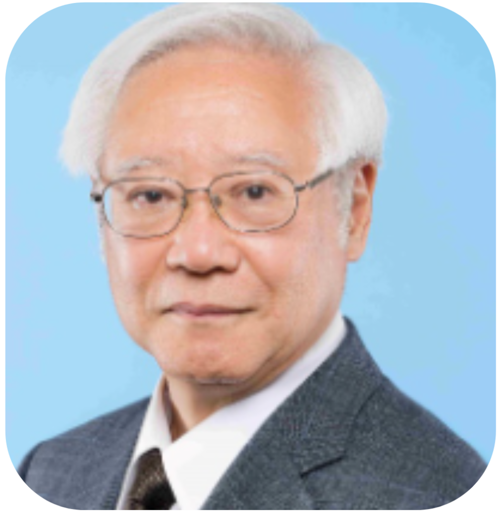
Hiroshi Iwai is a semiconductor device engineer who contributed to the development of LSI products and their technologies for 50 years since 1973 at Toshiba Corporation, Tokyo Institute of Technology, and National Yang Ming Chiao Tung University. He is an Eminent Lecturer of IEEE Electron Devices Society and a committee member of IEEE IRDS (International Roadmap for Devices and Systems).

Abstract
Over the last decade, the cost of photovoltaic solar energy conversion has dropped very dramatically with solar photovoltaics “now the cheapest source of electricity in most countries” and “now offering some of the lowest cost electricity ever seen”, according to the International Energy Agency. However, improvements are in the pipeline that are leading to an era of “insanely cheap” solar power, within the coming decade. The developments leading to these cost reductions will be described as well as the pending improvements that will allow solar to continue on its trajectory to even lower future costs over the 2020-2030 decade.
Biography
Martin Green is Scientia Professor at the University of New South Wales, Sydney and Director of the Australian Centre for Advanced Photovoltaics, involving five other Australian Universities and research groups. His group’s contributions to photovoltaics include inventing the PERC cell, now accounting for 90% of global production, and holding the silicon solar cell efficiency record for 30 of the last 38 years, regarded as a “Top Ten” milestone in solar photovoltaics history. Major international awards include the 1999 Australia Prize, the 2002 Right Livelihood Award, also known as the Alternative Nobel Prize, and most recently, the 2021 Japan Prize.

Abstract
Packaging is undergoing a major paradigm shift and promises to take up the lag caused by the slowing down of CMOS scaling. In this paper, we examine these shifts that have been driven by the scaling of key packaging metrics such as bump pitch, trace pitch, inter-die spacing and alignment. The goal of advanced packaging is to enable the same benefits that Moore/Dennard scaling has accomplished for CMOS viz. density, performance, power, and cost. The vehicles that advanced packaging employs are somewhat different: dielets/chiplets, advanced assembly techniques, simplified inter-chip communication protocols and cost optimization via the use of optimized heterogeneous technologies. Another important aspect of advanced packaging is the adoption and adaptation of silicon technology methods to packaging.
In this talk we will discuss the technologies and some instantiation examples that we have developed at UCLA.
Biography
Subramanian S. Iyer (Subu) is Distinguished Professor and holds the Charles P. Reames Endowed Chair in the Electrical Engineering Department and a joint appointment in the Materials Science and Engineering Department at the University of California at Los Angeles. He is Director of the Center for Heterogeneous Integration and Performance Scaling (UCLA CHIPS). Prior to that he was an IBM Fellow. His key technical contributions have been the development of the world’s first SiGe base HBT, Salicide, electrical fuses, embedded DRAM and 45nm technology node used to make the first generation of truly low power portable devices as well as the first commercial interposer and 3D integrated products. He also was among the first to commercialize bonded SOI for CMOS applications through a start-up called SiBond LLC. More recently, he has been exploring new packaging paradigms and device innovations that may enable wafer-scale architectures, in-memory analog compute and medical engineering applications. He has published over 300 papers and holds over 75 patents. He has received several outstanding technical achievements and corporate awards at IBM. He is an IEEE Fellow, an APS Fellow, an iMAPS Fellow and a Distinguished Lecturer of the IEEE EDS and EPS and a member of the Board of Governors of IEEE EPS. He is also a Fellow of the National Academy of Inventors. He is a Distinguished Alumnus of IIT Bombay and received the IEEE Daniel Noble Medal for emerging technologies in 2012 and the 2020 iMAPS Daniel C. Hughes Jr Memorial award and the iMAPS distinguished educator award in 2021.


