Invited Speakers
Biography
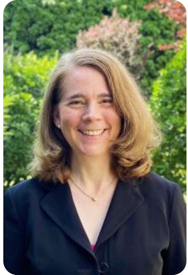
Dr. Laurie Calvet received a BS in Applied Physics from Columbia University (1995) and MS (1996), M.Phil. (1998) and a Ph.D. (2001) in Electrical Engineering from Yale University. Here thesis work explored electronic transport in silicon Schottky barrier transistors. During her post-docotral studies she studied how chemically synthesized materials can be used in electronic devices. In 2006, she joined the Centre de Nanosciences and Nanotechnologies (formerly the Institut d’Electronique Fondamentale), as a post-doc and in 2007 she was recruited into the French CNRS. Her current research explores how to realize energy efficient devices and architectures that are inspired from biological systems. One research topic focuses on using organic electronics, which promises low cost low carbon footprint devices, for use in neuromorphic devices. The goal of this numerical work is to show how to realize full classification circuits in a completely organic technology.

Biography
Theresia Knobloch is a postdoctoral researcher focusing on fabrication, experimental characterization, design, and modeling of nanoelectronic devices based on 2D materials. She received her doctoral degree from TU Wien in 2021 and performed parts of her Ph.D. research as a visiting scholar at Purdue University, USA in 2018 and 2019 and Soochow University, China in 2017. For her work, she received several awards including the IEEE EDS Ph.D. Student Fellowship in 2021 and the Best Student Paper Award at the DRC in 2020. She joined the Institue for Microelectronics in 2016 while completing her master’s degree in microelectronics and photonics. She received both her M.Sc. in 2016 and her B.Sc. in technical physics in 2014 from TU Wien with distinction. Currently, she primarily studies the electrical stability and reliability of 2D material-based field-effect transistors and focuses on the role of the gate insulator.
Abstract
Field-effect transistors (FETs) based on two-dimensional (2D) materials are a promising candidate for ultrascaled transistors towards the end of the roadmap. When using 2D materials as atomically thin channels, they improve gate control while simultaneously maintaining sizable mobilities. Furthermore, 2D materials can be monolithically integrated with silicon CMOS chips to enhance their functionality by building integrated photonic circuits, neuromorphic computing arrays or sensor elements, nanoelectronic devices often based on metal-insulator-semiconductor (MIS) systems. Thus, in recent years considerable research efforts have explored various 2D semiconductors as channel materials for FETs. However, up to now the key challenge of identifying scalable and reliable gate insulators for 2D materials has received little attention. First, suitable gate insulators need to be scalable to sub-1nm equivalent oxide thicknesses without resulting in excessive gate leakage currents. Second, for competitive device performance, insulators need to provide low densities of interface traps and insulator traps and should offer a high dielectric strength. Third, suitable processes for insulator deposition on top of 2D semiconductors need to be developed. In general, amorphous oxides like hafnium oxide, aluminum oxide or silicon dioxide are typically used as insulators for 2D semiconductors and also the layered insulator hexagonal boron nitride is regularly used. However, this talk will address why the aforementioned insulators are likely unsuitable for scalable, reliable 2D FETs and will examine more exotic insulators which show promise including calcium fluoride, muscovite mica or bismuth selenite.
Biography
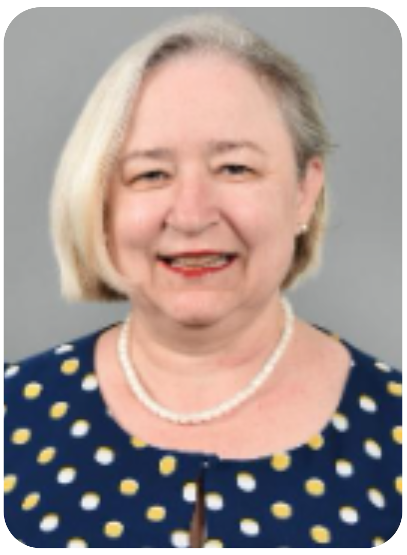
Dragica Vasileska is a Professor of Electrical Engineering at Arizona State University: She received B.S.E.E. and M.S.E.E. Degree from the University Sts Cyril and Methodius (Skopje, Republic of North Macedonia) in 1985 and 1991, respectively, and a Ph.D. Degree from Arizona State University in 1995. Her research interests include semiconductor device physics and semiconductor device modeling, with strong emphasis on quantum transport and Monte Carlo device simulations. Recently, her research interests also include modeling metastability and reliability of solar cells. Prof. Vasileska published in prestigious scientific journals, conference proceedings, has given numerous invited talks and is a co-author on three books: “Computational Electronics,” D. Vasileska and S. M. Goodnick, Morgan & Claypool, 2006; “Computational Electronics: Semiclassical and Quantum Transport Modeling,” D. Vasileska, S. M. Goodnick and G. Klimeck, CRC Press, 2010, and “Modeling Self-Heating Effects in Nanoscale Devices,” K. Raleva, A. Shaik, D. Vasileska and S. M. Goodnick, Institute of Physics Publishing, Morgan & Claypool, 2017. She is also an editor of two books: “Cutting Edge Nanotechnology,” In-Tech, 2010 and “Nano-Electronic Devices: Semiclassical and Quantum Transport Modeling” (co-editor S. M. Goodnick), Springer, July 2011. Prof. Vasileska is a recipient of the 1998 NSF CAREER Award. Her students have won numerous awards at prestigious international scientific conferences.
Abstract
Modeling and simulation is the third alternative to theory and experiments. It is cheaper, faster and provides insight into physical processes occurring within the device that cannot be measured experimentally. As such, modeling and simulations reduces the time from design to production of a particular device and/or circuit. In this talk, I will present a summary of the available simulation methodologies and products: commercial TCAD tools, nanoHUB platform and few examples of in-house simulation tools that have not yet been adopted by the TCAD community.

Biography
Dr. Fernando Guarín is a Distinguished Member of Technical Staff at Global Foundries in East Fishkill New York. He retired from IBM’s SRDC after 27 years as Senior Member of Technical Staff. He earned his BSEE from the “Pontificia Universidad Javeriana”, in Bogotá, Colombia, the M.S.E.E. degree from the University of Arizona, and the Ph.D. in Electrical Engineering from Columbia University, NY He has been actively working in microelectronic reliability for over 40 years.
From 1980 until 1988 he worked in the Military and Aerospace Operations division of National Semiconductor Corporation. In 1988 he joined IBM’s microelectronics division where he worked in the reliability physics and modeling of Advanced Bipolar, CMOS and Silicon Germanium BiCMOS technologies. He is currently leading the team qualifying GlobalFoundries RF 5G technology offerings.
Abstract
As new fifth generation (5G) radio cellular networks operating in the mmWave frequency enter the market there is an increased need for stress and test methodologies for devices and circuits operating at or above 28GHz[1].The reliability evaluation for Silicon On Insulator (SOI) technologies requires new methods for stress and characterization to guarantee suitable lifetimes to make them feasible solutions for next generation cellular networks, satellite communications and IoT applications.
Biography
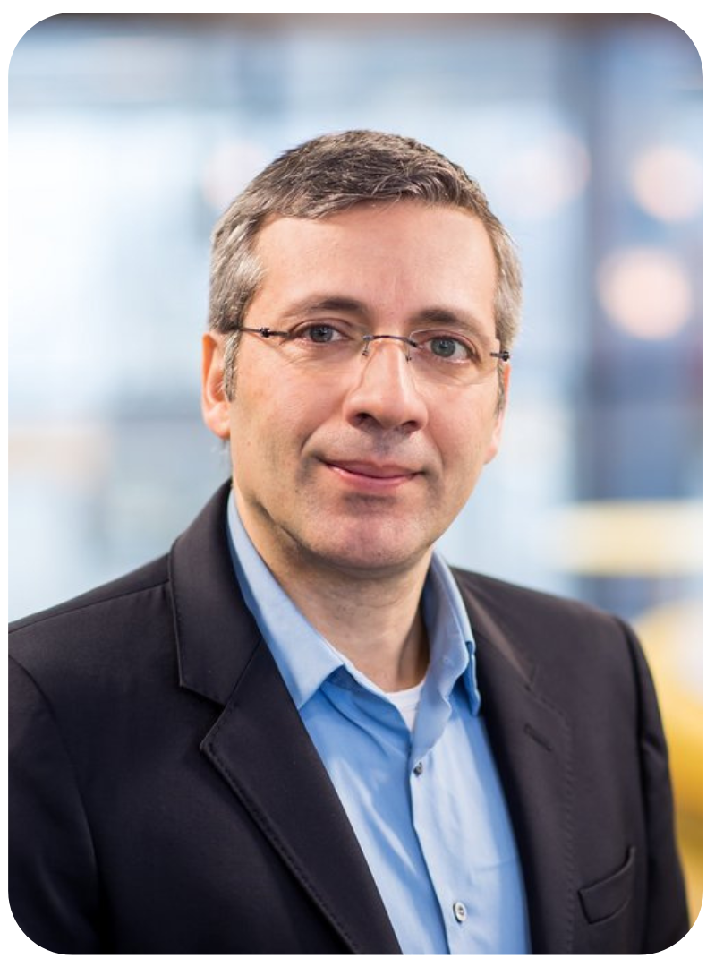
Eugenio Cantatore received his Master’s and Ph.D. Degree in Electrical Engineering from Politecnico di Bari, in 1993 and 1997 respectively. Till 1999 he was fellow at the European Laboratory for Particle Physics (CERN), Geneva. In 1999 he moved to Philips Research, Eindhoven, and in 2007 joined the Eindhoven University of Technology, where he is full professor since 2016. His research interests include the design and characterization of electronic circuits exploiting emerging technologies and the design of ultra-low power integrated systems. He authored or co-authored more than 200 papers in journals and conference proceedings, and 13 patents. He has been active in the Technical Program Committees of ESSDERC, IWASI, ESSCIRC and ISSCC. At ISSCC he has been chair of the Technology Directions subcommittee, Program Chair in 2019 and is presently Conference Chair. He has been member at large of the SSCS AdCom, associate editor of the IEEE Transactions on Circuit and Systems I and is now editor in chief of the IEEE Open Journal of the Solid-State Circuits Society. In 2006 he received the ISSCC Beatrice Winner Award for Editorial Excellence and was nominated in the Scientific American top 50 list. He received the Philips Research Invention Award in 2007, the Best Paper Award from ESSDERC 2012 and the Distinguished Technical Paper Award from ISSCC 2015. He was nominated IEEE Fellow in 2016.
Abstract
Flexible sensing surfaces are the next frontier in large area electronics. Integrating sensors and electronics on flexible substrates it is possible to create surfaces that are capable of mapping the distribution of several quantities of practical interest: from pressure to X-rays, and from biopotentials to the infrared radiation generated by warm objects. In this paper we overview the main approaches and challenges in this field of research, focusing especially on solutions manufactured using organic materials.

Biography
Gilson Wirth received the B.S.E.E and M.Sc. degrees from the Universidade Federal do Rio Grande do Sul, Brazil, in 1990 and 1994, respectively. In 1999 he received the Dr.-Ing. degree in Electrical Engineering from the University of Dortmund, Dortmund, Germany.
He is currently a professor at the Electrical Eng. Depart. at Univ. Federal do Rio Grande do Sul – UFRGS (since January 2007).
From July 2002 to December 2006 he was professor and head of the Computer Engineering Department, Univ. Estadual do Rio Grande do Sul – UERGS.
His current research work focuses on modeling and electrical stimulation of charge trapping in the context of Bias Temperature Instability (BTI), Low-Frequency Noise (1/f and RTN) and Hot Carrier Degradation (HCD).
He has also worked on ionizing radiation effects (TID and SET/SEU) on semiconductor devices.
He focuses on collaborative work with academia and industry. He has stablished successful collaborative work with different companies and research groups in Europe, North and South America, and China.
He is currently a Distinguished Lecturer of the IEEE Electron Devices Society. He also was a distinguished lecturer of the IEEE Circuits and Systems Society (term 2010-2011).
An updated list of publications may be found at http://lattes.cnpq.br/1745194055679908
Or https://publons.com/researcher/3063393/gilson-wirth/
Abstract
Random Telegraph Noise (RTN) causes the drain current (or threshold voltage) of a MOSFET to randomly vary over time.
We discuss estimators for the variance and variance of variance of the RTN – drain current or threshold voltage – as a function of the observation time window. The observation time window may be limited by the circuit or measurement setup bandwidth, as well as by the duration time of the observation.
Both intra device variance as well as inter device variance are discussed. Intra device variance refers to the variance of the observed RTN for different time periods – different time windows – in a single device. Due to the stochastic RTN nature, behavior observed in a single device may be different at different observations. This intra device variance is modeled and it is show how it can be used to extract trap time constants, and possibly as an estimator for number of active traps in a device.
Also, RTN behavior of devices of same size – designed to be identical – are going to differ, due to different number of traps and different trap properties. This is related to inter device variance. This inter device variance is also modeled and it is show how it can be used to extract relevant statistical parameters for noise modeling, which can be used for circuit analysis in both time and frequency domains.
At circuit level, it is discussed how RTN induces stochastic timing variations in nanometric CMOS logic gates, as well as jitter and phase noise in oscillators. It is also show that, compared to the case of white noise, with charge trapping oscillator jitter grows faster with elapsed time.
Keywords: Charge Trapping, Random Telegraph Noise, Time Dependent Variability, Phase Noise, Jitter.

Biography
Dr. Kun graduated from the Merchant Marine Academy in Uruguay and holds a BSEE; MSEE and Ph.D. degree in BME all from UCLA. He is a Distinguished Professor Emeritus of National Security Affairs (CHDS) and was Professor of Homeland Security at the National Defense University (2003-2015). A (Lifetime) Fellow of the IEEE, the American Institute for Medical and Biological Engineering, the International Academy of Medical and Biological Engineering and the International Union for Physical and Engineering Sciences in Medicine. He was founding Editor in Chief of Springer’s Journal of Health and Technology 2010-2020. He spent 14 years at IBM and later Director of Medical Systems Technology at Cedars Sinai Medical Center. As Senior IT Advisor to AHCPR he formulated the IT vision and was the lead staff for High Performance Computers and Communications program and Telehealth. In July 1997, as invited speaker to the White House, he was largely responsible for the first Telemedicine Homecare Legislation signed by President Clinton, August 1997. While a Distinguished Fellow at the CDC, as Acting Chief IT Officer for the National Immunization Program he formulated their IT vision on 10/2000. Kun received many awards including: AIMBE’s first-ever Fellow Advocate Award in 2009; IEEE-USA Citation of Honor Award, “For exemplary contributions in the inception and implementation of a health care IT vision in the US.” 2011 Golden Core Award by the IEEE Computers. Named: “Profesor Honoris Causa” by Favaloro University, (2009); “Distinguished Visitor” by City of Puebla, (Mexico 2013). He is/was an EEE Distinguished Lecturer for Computer Society, Engineering in Medicine and Biology Society and Chairman for SSIT’s DL Program. Kun is an Honorary Professor of the Electrical Engineering Dept. at the School of Engineering of the University (UDELAR) in Montevideo, Uruguay. He received the Medal of Merit in 2016 in Mexico by the National Unit of Engineering Associations and named Visiting Professor by the National Technological University of Buenos Aires, Argentina, November 2017.
Abstract
While the world struggled with COVID-19, it was expected that primary, secondary and college students would attend school via distance learning, while people would telework and the public would access their medical support via telemedicine. In addition, purchases of products would be done (mainly) via e-Commerce. These assumptions may be clear for the developed world, however approximately 60% of the world does not have Internet access and if additionally, you lack safe drinking water, food, health or a house to live in, Internet is not a priority. The Information Age is providing data that shows in real time complexity and the lack of interoperability among global participants. In the Global Economy, Society lives in silos. While the world faces simultaneously a large number of interrelated challenges, different governments are trying unsuccessfully to address them not as a complex dynamic system but as independent and separate ones. According to a 2022 Global Risks Survey,20% the world population lives in 52 of the poorest countries and only 6% have been vaccinated against COVID-19. The water crisis and the WHO/UNICEF: 2.2 billion lack access to clean drinking water and sanitation. Approximately 1 million people die every year from hygiene-related diseases such as: diarrhea, cholera, dysentery, typhoid, and polio, all preventable. The world is currently trying to deal with the COVID-19 pandemic, climate change, the water and food crisis and contemplating a potential famine for millions living in very poor countries as a result of an ongoing war between Russia and Ukraine that prevents them from getting wheat, barley, corn and sunflower oil. If we look at the US as microcosm of the world, for most educated people, political polarization / midterm elections, mass shootings and the unrestricted sale of guns with no background checks, race, the price of gasoline, food and the cost of living are the “current” big worries. For years, areas such as California’s San Joaquin Valley have been booming their agricultural industry while confronting punishing droughts and fires, due to climate change, leading to water over-extraction from aquifers. This process is irreversible and the lands have sank 28 feet in a fairly short period of time. According to a 2021 Science article subsidence will affect 1.6 billion people who will be displaced in the next 2 decades because those areas will be susceptible to floods. Meanwhile Lakes Mead, Powell, Travis, Great Salt Lake and many others, are quickly disappearing and the water that would flow to California for agriculture purposes not only is disappearing but in some instances the minerals left below will make areas such as Salt Lake City unlivable. With the daily global population increases (perhaps reaching 10 billion by 2045), water, food and energy will be major challenges to the world. The February 2021 climate crisis in Texas, showed not only how all of our Critical Infrastructures are interdependent among themselves but how dependent we are with cyberspace, and how unprepared the world is for the effects of climate change. A new holistic transformational approach is needed, where biomedical / system engineers and or computer scientists help integrate the multidisciplines and interdisciplines needed to solve these challenges.
Biography
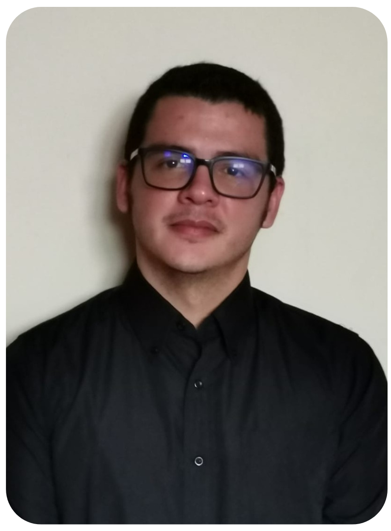
MsC in Electronic Engineering, Embedded systems from the Instituto Tecnológico de Costa Rica. Allan has over 10 years of experience working on the design, implementation, and programming of switching ASICs for Hewlett Packard Enterprise. Besides, Allan has been part of different research programs like the SpiderBot in 2010 focused on the investigation of a MEMS (microelectromechanical systems) device for autonomous movement. In 2016, he collaborated with engineers of the TUDelft University in the investigation of increasing the computing performance of small satellites (CubeSat).
Abstract
This Go-Modeling project is an effort to create and develop useful models that can be reviewed later for HW and SW implementations. The models are created using KPN-based networks which interact and share information for further exploration. This work focuses on the blocks of specification and model providing a simplified testing of the model and it is implemented in Go language which has several advantages in working with concurrent processes and interactions.
Each process implementation is given in the form of a Go package by the user. The main idea is that each process is a simple and concise function, optimize to execute a specific task. The user interconnects these processes using a YAML specification file which defines how these will interact. The modeling process oversees the auto-generation and validation of a customized version of a KPN model, which can be executed to review functionality and gather information on the model space exploration.
Having a functional behavior of the model and how the different processes interact can give the designers much information on how specific task behaves, and how the different components interact with each other. Also, as it is a KPN network, specific processes can be reviewed on how they consume tokens and the way they deliver its information to subsequent parts of the model.
Biography
Dr. Ricardo Donaton is a Senior Technical Staff Member in the IBM Quantum team working on quantum processor development, fabrication and delivery for quantum systems deployment. He currently leads the effort of developing new interconnects and packaging fab processes for quantum computing applications, bringing them from research into development. He has extensive experience in materials and semiconductor technology development from his work at IBM Semiconductor Research and Development Center and IMEC. He received his Ph.D. in Physics from IMEC / Katholieke Universiteit Leuven, Belgium in 1999.
Abstract
Quantum Computing is making its way from research laboratories to engineered quantum systems. It is moving from the “fantastic” to the practical. At the core of quantum computing is the hardware that enables quantum programs to be executed. IBM Quantum processors have been evolving by scaling the number of qubits, improving coherence times, gate fidelities and speed and our recent announced Quantum Development Roadmap plans to deliver a 4,000+ qubit quantum computer by 2025. We will discuss the evolution of our quantum processors, focusing on architectures integrating new technology elements such as multi-layer wiring, superconducting vias and advanced packaging techniques.

Biography
Dr. Stefan van Waasen is head of the Electronic Systems institute at Forschungszentrum Jülich in Germany since 2010 and Professor at Duisburg-Essen university in “Measurement and Sensor Systems” since 2014. He received his diploma and doctoral degree from Gerhard-Mercator University Duisburg in 1994 and 1999, respectively. He worked more than a decade at Infineon Technologies AG in product development for System-on-Chip solutions in communication system with focus on concept development and systems engineering.
His institute has the focus on research for complex electronic and information technology systems solutions taking the full potential of integrated circuits. Since some years there are two main efforts: on hand on the research for electronic systems for future scalable universal quantum computing in the sense of control/read-out up to as well as on the other hand identifying and implementing added value applications for memristive devices.
His personal interests are in system modelling as well as systems engineering for complex electronic systems and generating best synergies in both direction between academic research in combination with industrial development methods/targets.
Abstract
There is a huge ongoing hype on the vision of quantum computing (QC) in the science community with envision to enable access to “unsolvable” problems for HPC. Correspondingly there is grown and still continuing growing ecosystem for demonstrator developments with huge funding activities in many countries, also especially in Europe but also in industrial environment. Independent of the qubit technology in these great science projects for demonstrators do not really consider or only marginally touch the challenge on real system scaling to enable real universal QC with 1 million or more qubits. This requirement is not only driven out of the huge complexity for solving scientific problems but especially also from the needed error correction schemes.
This scaling challenge raises directly the question how to partition and where to place the classical control electronics. We in the Central institute of Engineering, Electronics and Analytics – Electronic Systems (ZEA-2) at Forschungszentrum Jülich try to tackle the challenge in this stage of the development with CMOS electronics also in direct vicinity of the qubits, so at temperatures below 1 K. Beside system and pure implementation aspects which will be presented, the influence of all CMOS devices itself have a huge influence. The behavior at cryogenic temperatures has to be fully considered in these aspects and for the future it will require further tremendous technology developments to make a full system solution possible. This talk will try to give a glance on some of these topics.

Biography
Dr. David H. Hughes is a senior researcher in the Department of Astrophysics at the Mexican National Institute of Astrophysics, Optics and Electronics (INAOE). He received his Ph.D. in Astrophysics from the University of Central Lancashire, England in 1990. Following post-doctoral studies at the Universities of Oxford and Edinburgh, he moved to Mexico in 1999 to contribute to the advancement of millimeter-wavelength astronomy and the technical and scientific development of the Large Millimeter Telescope Alfonso Serrano (LMT) and its instrumentation program. Since 2011 he has served as the binational (Mexico/USA) Director of the LMT. He has published more than 200 peer-reviewed papers related to the formation and evolution of galaxies and their active nuclei. He is a co-discoverer of the “sub-millimeter galaxy population, SMGs” that represents the most massive and active star-forming galaxies that exist in the early universe. He is a member of the Mexican Academy of Sciences and has been awarded a number of national recognitions including the Mexican Puebla State Luis Rivera Terrazas prize for Science and Technology in 2019. Dr. Hughes is currently the vice-Chair of the governing Board of the global Event Horizon Telescope (EHT) collaboration and the leader of the Mexican participation in the EHT project. In April 2019, the EHT collaboration presented the first image of the shadow (the event horizon) of a supermassive black hole which received wide worldwide recognition by the public sector and the international scientific community. As a member of the Event Horizon Telescope collaboration, Dr. Hughes has been the recipient of multiple international honors including the Breakthrough Prize 2020 in Fundamental Physics, Royal Astronomical Society Group Award 2020, Einstein Medal 2020, American Astronomical Society Bruno Rossi Prize 2020 and the National Science Foundation Diamond Achievement Award 2019.
Abstract
The global Event Horizon Telescope collaboration, including the participation of the Large Millimeter Telescope Alfonso Serrano (LMT) and members of the Mexican research community, has recently reported the first ultra-high angular-resolution observations of the super massive black-hole, SgrA*, in the nucleus of our galaxy, the Milky Way.
The published image clearly shows a central shadow surrounded by a ring of light, an image consistent with the predictions of the law of general relativity published by Albert Einstein in 1915. In particular the image confirms the existence of a “singularity” and the creation of a black-hole with a mass of approximately 4 million times the mass of our sun. I will describe the scientific impact of this first “photo” of the super massive black-hole in SgrA* and summarise how Very Long Base-line Interferometric (VLBI) observations, conducted at a wavelength of 1.3mm with the international Event Horizon Telescope, were able to create a synthetic telescope with a size approximately equal to the diameter of the earth. This presentation will conclude with a summary of the contribution of the LMT and Mexico to these unique world-class results and the future technical evolution of the Event Horizon Telescope experiment.
Biography
Fernando Silveira received the Electrical Engineering degree from Universidad de la República, Uruguay in 1990 and the MSc and PhD in Microelectronics from Université catholique de Louvain, Belgium in 1995 and 2002. He is currently Professor at the Electrical Engineering Department of Universidad de la República. His research interests are in the design of ultra-low-power analog and RF integrated circuits and systems, in particular with biomedical application. He is coauthor of two books and many technical articles. He has had multiple industrial activities, including leading the design of an ASIC for implantable pacemakers and designing modules for implantable devices for various companies worldwide. He is a senior member of IEEE and served as IEEE CASS Distinguished Lecturer (2011 – 2012), Associate Editor of IEEE TCAS II (2020 – 2021) and member of Senior Editorial Board of JETCAS (2022 – 2023).
Abstract
Traditionally the reliability dimension is handled at the design level as an issue of keeping operation (voltage, current) within fixed boundaries (e.g., the safe operating area). These boundaries are defined at the device and process level. As a general process specification, they are defined taking care of covering a broad range of circuits and operation regimes, as well as assuring minimum device degradation Reliability is pre-assured to, statistically, be within certain range once the general operating conditions are respected and it is decoupled from the design process. This is a sensible approach that simplifies the designer task since, except for respecting these boundaries, no other consideration needs to be taken regarding reliability. Nevertheless, this comes with a cost. Since the operating boundaries are defined in a general context, they are excessively restrictive in particular cases and hinder the achievable performance. Additionally, being defined to assure minimum device aging, they do not take advantage of techniques at the design level, from very simple to more complex ones, that can preserve performance with aging by introducing resilience and adaptation to device degradation. By including reliability as an additional performance parameter to be taken care during the design process, i.e., following a reliability aware design process, our circuits can age gracefully and simultaneously improve the performance.
Biography
Sebastian Matias Pazos received his degree in Electrical Engineering in 2015 and his PhD in 2021 by Universidad Tecnólogica Nacional, Facultad Regional Buenos Aires (UTN.BA), Argentina. He received fellowships from DAAD, UTN.BA and CONICET and was Interim Professor and TA at UTN.BA. He is currently a Post-Doctoral Fellow at King Abdullah University of Science and Technology (KAUST), Saudi Arabia, and member of the EDS Nanotechnology Committee. He co-authored more than 20 articles in international journals and was co-awarded 3 best paper awards in international conferences. His interests include CMOS RF/AMS circuit design, advanced materials integration, device/circuit reliability and neuromorphic hardware.
Abstract
A design for reliability approach is proposed for fully integrated RF CMOS class A-to-C power amplifiers. Reliability hazards like time dependent dielectric breakdown and hot carrier injection are mapped into the design space, including the expected parametric degradation of the circuit, by fitting widely accepted models to experimental degradation results on the target technology. A prototype amplifier was used to validate RF degradation models and their impact on the output power degradation under accelerated stress. The methodology is based on a design space exploration of the highest efficiency designs attainable in a target technology. Electrical characteristics of passives and transistors are considered through look-up tables. The proposed approach allows to reduce the full universe of available designs to those that are specification and reliability compliant, avoiding a simulator-in-the-loop approach. A test case for a 3 dBm output power amplifier from the design space shows good agreement between predictions and SPICE simulations, including projected parametric degradation due to hot carrier injection.
Biography
Pascal XAVIER, was born in France in 1964. He received the Ph. D. degree in Physics from the University of Grenoble, France, in 1994. He was also graduated from Grenoble INP in electrical engineering in 1988. From 1994 to 2003, in the CNRS, his research interests were dealing with numerical methods for the analysis of coupled thermo-electromagnetics problems and design of microsensors in the fields of microwaves.
He joined the Research Institute of Microelectronics, Electromagnetism and Photonics (IMEP-LaHC) of Grenoble in 2003 where he is currently the leader of the “DHREAMS” team. His research interests include design, realization and test of sustainable microwave devices and sensors for environmental applications, bioelectromagnetism and characterization of complex materials.
He is Professor in the Department of Electrical Engineering, Technology University Institute of Grenoble, involved in teaching of Electronics and Physics and is currently responsible of the specialty « Optics and RF » in the Doctoral School EEATS of the Grenoble Alps University (UGA).
Abstract
Like other sciences and technologies, electronics today faces an enormous challenge due to the scarcity of non-renewable resources and the need to decrease greenhouse gas emissions in order to reduce the climate change. In this context, the search for alternative roadmaps at all stages of the life cycle of an electronic product is a major issue. Additive processes, bio-sourced or organic materials and recyclable substrates are examples of subjects that can be explored to progressively substitute high impacts materials and methods by eco-friendly ones. At the same time, these solutions have a number of shortcomings that must be overcome in order for them to become economically and technically credible. In the domain of radio frequency devices, paper printed antennas and filters, electromagnetic energy harvesting systems, sensors and displays can be designed. This article presents an overview of what has been undertaken in this field by our team for over ten years for the design, fabrication and test of antennas. These devices were tested in several real environments for different applications such as anti-counterfeiting.
Biography
Dr. Khandelwal leads a vibrant research group at Macquarie University focussing on semiconductor device modeling and simulations. He is the lead author of world-wide industry standard ASM-HEMT model for GaN RF and power devices at the CMC. He has authored over 150 papers, and published 3 books on the subject covering GaN, FDSOI, and FinFET technologies.
Prior to this role, Dr. Khandelwal was with BSIM group at the University of California Berkeley, and IBM Semiconductor Research Center.
Biography
Christoph Jungemann (Fellow, IEEE) received the M.Sc. (Dipl.-Ing.) degree and the Ph.D. (Dr.-Ing.) degree in electrical engineering from the RWTH Aachen University, Aachen, Germany, in 1990 and 1995, respectively.
He worked at the R&D department of Fujitsu, Kawasaki, Japan, from 1995 to 1997, and was a senior engineer at the University of Bremen, Bremen, Germany from 1997 to 2002, where he received the venia legendi for electromagnetic theory. He spent a year at the Center for Integrated Systems of the Stanford University, USA, as a research associate. In 2003 he joined the Technical University of Braunschweig, Germany, as a researcher and became a professor at the University of the Armed Forces in Munich, Germany, in 2006, where he held the chair for microelectronics until 2011. Since 2011 he is a professor for electromagnetic theory at the RWTH Aachen University and head of the institute of electromagnetic theory. From 2017 until 2021 he served as dean of academic affairs of the Faculty of Electrical Engineering and Information Technology of the RWTH Aachen University. He was a co-recipient of the IEEE Paul-Rappaport-Award for 2005. From 2007 until 2010 he was an editor of the IEEE Transactions of Electron Devices. In 2017 he received the RWTH Aachen University Award for excellence in teaching. He has published two books, three book chapters and more than 250 articles in scientific journals and conference proceedings. His research focuses on the development of simulation approaches for charge transport in semiconductor devices including electronic noise, THz waves, device degradation and organic materials.
Abstract
Dyakonov and Shur suggested electron-plasma instabilities in the channel of HEMTs as new sources for THz waves that could fill the THz gap. Their analytical model was based on the Euler equation and Dirichlet boundary conditions for the electron density at the source side of the channel and for the current density at the drain side. There have been many attempts to solve the equations for realistic devices by numerical simulation, where the boundary conditions between the channel and the highly doped source/drain regions (ohmic contacts) are a result of the device simulations. The only boundary conditions, that can be specified in the device simulations are the ones between the highly doped regions and the terminals. It turned out that these boundary conditions have a strong impact on the plasma resonances in the HEMT and the resonances vanish, if the device is simulated by the more physics-based Boltzmann transport equation in conjunction with thermal bath boundary conditions. The lack of plasma instabilities in these simulations is matched by experiments, in which no clear indications of instabilities could be found.
Biography
Hans obtained his diploma in physics from the University of Jena in 2009. From 2009-2012 he joined Prof. Leo’s group at Technische Universität Dresden where he was focusing organic electronics. After having received his PhD in 2013 from TU Dresden, Hans joined NOVALED/ Samsung SDI as a researcher/ project-leader on organic transistors for display applications. He returned to academia in 2016 and joined the group of Prof. Dr. Feng Wang at the Physics Department of UC in Berkeley, USA. In 04/2017, Hans started as a group leader at TU Dresden where he is focusing on next level organic electronic devices. In 2021 he received a Habilitation from TU Dresden.
Abstract
The vision of flexible electronics based on organic semiconductors is to enable lightweight, cost effective, power-efficient, and versatile electronic devices that can support people in any aspect of life. In this regard, organic thin-film transistors (OTFTs) that can operate at low voltage (<5.0 V), possess high on/off ratios (>10 6), and work at high frequencies are required to turn this vision into reality. However, lateral transistor configurations face severe contact resistance and device integration challenges when targeting short-channel geometries (L<3μm), which are required to reach device operation above 100MHz.
In this contribution, I will discuss the idea of employing vertical organic transistors – a structure that holds great promise for high-frequency applications as the channel length is defined only by the thicknesses of the layers in these devices and hence can be as low as 100nm. As an archetype device, I will focus on so-called organic permeable base transistors to explain the device physics and scaling laws of vertical organic transistors. In addition, I will present the first organic bipolar junction transistor, which utilizes the vertical organic transistor configuration. Although the intrinsic gain of such devices is still much lower than in organic permeable base transistors, the fast recombination processes in bipolar transistor devices offer device operation above the GHz-threshold.

Biography
François Danneville received the PhD in Electronics and the «Habilitation à Diriger les Recherches » from Lille University, in 1991 and 1999, respectively. In 1998, he made one year sabbatical as Visitor Scientist in HP (nowadays Keysight Technologies), Santa Rosa (USA). Since 2001, he has been Professor at Lille University where his research has focused on the small (large) signal and noise properties in high frequency range (RF-mmW) of advanced Silicon Technologies (CMOS and SiGe HBTs).
Since 2014, his research work has also focused on the development of an ultra-low power (ULP) neuromorphic technology (NT); in this framework, he is co-inventor of 3 patents (ultra low power artificial neuron/synapse/retina, standard CMOS, low voltage operation < 400 mV). He is currently working towards the use of this ULP NT in smart bioinspired visual and acoustic sensors for embedded systems. He has published over 170 papers in international journals and conferences and has supervised 27 PhD students (3 on-going).
Abstract
Applications in millimetre wave range and terahertz frequencies keep on increasing. In this context, drastic challenges are faced at measurement level, in particular to extract noise performance and nonlinear properties of devices and circuits used to build the required systems. The aim of this talk is to provide an overview of these challenges, and to describe the solutions that we have developed to respond to them.


