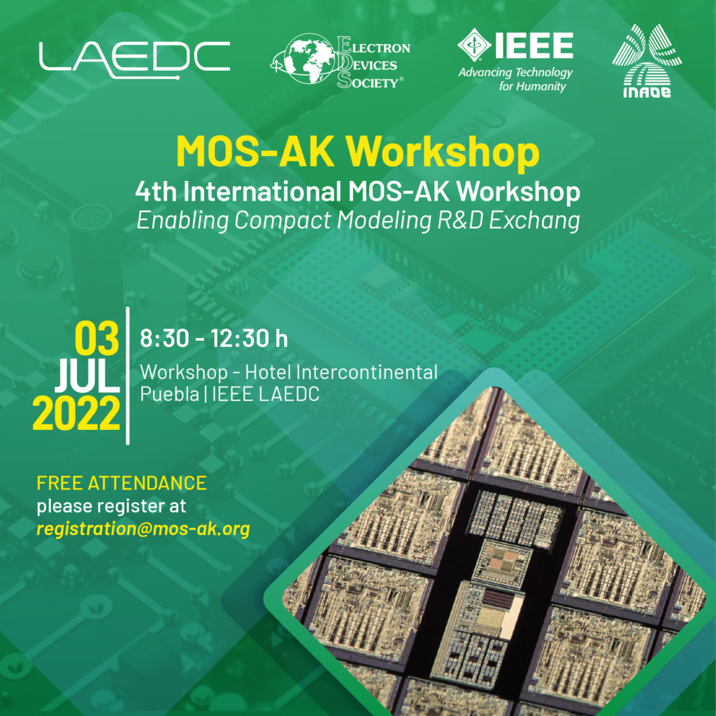
4th International MOS-AK/LAEDC Workshop
Enabling Compact Modeling R&D Exchange
In-person sessions will take place at the Intercontinental Hotel in Puebla. Máximo Serdán room.


- MOS-AK: July 3 2022, Puebla (MX)
- 8:30am – 12:30pm Workshop
Registration is FREE! Any related enquiries can be sent to registration@mos-ak.org
Abstract submissionis open; any related enquiries can be sent to abstracts@mos-ak.org
- HiTech forum to discuss the frontiers of electron device modeling with emphasis on simulation-aware compact/SPICE models and its Verilog-A standardization.
- MOS-AK Meetings are organized with aims to strengthen a network and discussion forum among experts in the field, enhance open platform for information exchange related to compact/Spice modeling and Verilog-A standardization, bring people in the compact modeling field together, as well as obtain feedback from technology developers, circuit designers, and CAD tool vendors. The topics cover all important aspects of compact model development, implementation, deployment and standardization within the main theme – frontiers of the compact modeling for nm-scale MEMS/NEMS designs, CMOS/SOI and HEMT IC simulation.
- The specific workshop goal will be to classify the most important directions for the future development of the electron device models, not limiting the discussion to compact models, but including physical, analytical and numerical models, to clearly identify areas that need further research and possible contact points between the different modeling domains. This workshop is designed for device process engineers (CMOS, SOI, BiCMOS, SiGe, GaN, InP) who are interested in device modeling; ICs designers (RF/Analog/Mixed-Signal/SoC/Bio/Med) and those starting in that area as well as device characterization, modeling and parameter extraction engineers. The content will be beneficial for anyone who needs to learn what is really behind the IC simulation in modern device models.
Topics to be covered include the following:
- Advances in semiconductor technologies and processing
- Compact Modeling (CM) of the electron devices
- Verilog-A language for CM standardization
- New CM techniques and extraction software
- Open Source FOSS TCAD/EDA modeling and simulation
- CM of passive, active, sensors and actuators
- Emerging Devices, CMOS and SOI-based memory cells
- Microwave, mmW, RF device modeling, high voltage device modeling
- Microsystems, SoC, IP modeling
- Device level modeling for Bio/Med applications
- Nanoscale semiconductor devices/circuits and its reliability/ageing
- Technology R&D, DFY, DFT and IC Designs
- Foundry/Fabless Interface Strategies


